
1/2
AN1768
APPLICATION NOTE
Æ
ADMISSIBLE AVALANCHE POWER OF SCHOTTKY DIODES
October 2003 - Ed: 1
D. JOUVE
INTRODUCTION
The design of Switch Mode Power Supply (SMPS) is subjected to ever increasing cost and efficiency
constraints.
One way to respond to these aggressive specifications is to use components closer to their intrinsic limits.
The increasing use of Schottky diodes in the avalanche area is a good example of this evolution.
To help the designer to optimize the choice of the Schottky diode in a rectification application,
STMicroelectronics is proposing a simple tool to determine if a given ST Schottky diode can withstand the
avalanche energy fixed by the application conditions.
0
0.2
0.4
0.6
0.8
1
1.2
25
50
75
100
125
150
175
Tj (∞C)
P
(t , T ) / P
(tp, 25∞C) versus T
ARM p
j
ARM
j
Fig. 2: Avalanche power derating over tempera-
ture range.
1. DESIGN RULES
The first step for the designer is to estimate, in the
worst-case conditions, the following parameters:
n
Operating junction temperature: Tj
n
Pulse duration of the avalanche current: tp
n
Avalanche energy by pulse generated by the
converter in the Schottky diode: E
AP
STMicroelectronics guarantees for each Schottky
diode a reference avalanche power given at
tp=1µs and Tj=25∞C: P
ARM
(1µs,25∞C) (corre-
sponding to a rectangular current pulse ).
Table 1 gives P
ARM
(1µs,25∞C) for some part
numbers.
Part number
P
ARM
(1µs; 25∞C)
per diode
STPS1545D (2x7.5A)
2.7 kW
STPS2045CT (2x10A)
4 kW
STPS3045CT (2x15A)
6 kW
STPS20H100CT (2x10A)
10.8 kW
Table 1: P
ARM
(1µs, 25∞C) values for some ST
Schottky diodes.
Derating curves
figure 2 and figure 3 give the ad-
missible avalanche power versus tp and Tj.
P
ARM
(1µs, 25∞C) for each part number as well as
the derating curves are given in the respective
datasheet.
The designer must ensure that the guaranteed
avalanche energy E
ARM
(tp,Tj) is greater than the
avalanche energy in the application E
AP
.
P
(t , T ) / P
(1µs,
) versus tp
ARM p
j
ARM
T
j
tp(µs)
10
1
1
0.01
0.1
0.1
0.001
0.01
100
1000
10
Fig. 3: Avalanche power derating over pulse dura-
tion range
AN1768 - APPLICATION NOTE
2/2
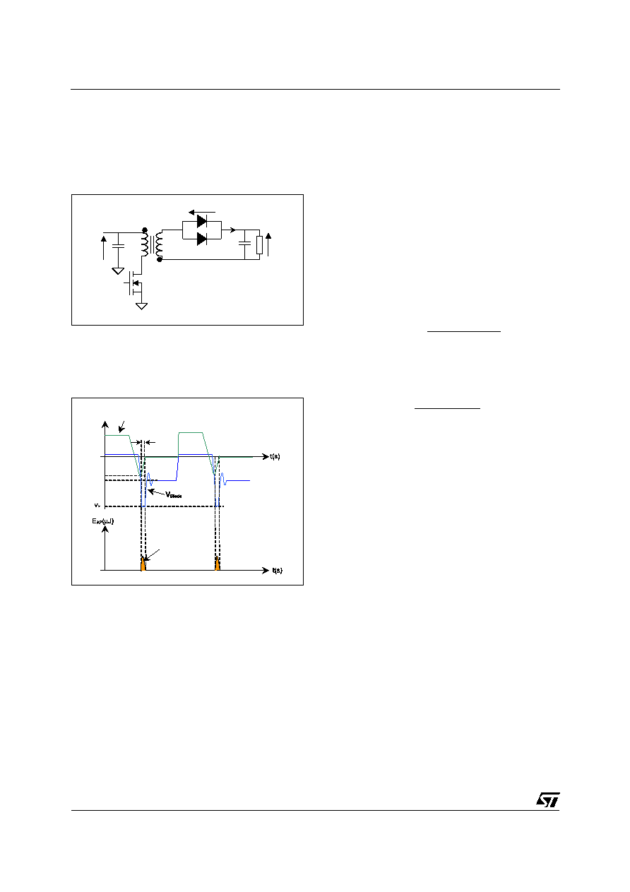
2. DESIGN EXAMPLE
Let us consider the use of a STPS20H100CT (two
10A, 100V ST Schottky diodes in TO-220 pack-
age) used in a flyback converter (
figure 4).
In a typical worst-case situation, the application
conditions are:
n
Operating junction temperature of the Schottky
diode:
Tj = 100∞C
n
Pulse duration of the avalanche current:
tp = 10ns
n
Avalanche energy by pulse through the two
diodes connected in parallel:
V
P
= -130V, I
AR
= -1.5A, tp = 10ns
E
AP
= 1.95µJ
∑
Table 1 gives:
P
ARM
(1µs, 25∞C)
STPS20H100CT
= 10.8 kW per diode
∑
Figure 2 gives:
P
tp
C
P
tp
C
ARM
ARM
(
,
)
(
,
)
.
100
25
0 45
∞
∞
=
P
ARM
(1µs,100∞C) = P
ARM
(1µs,25∞C) x 0.45
P
ARM
(1µs,100∞C) = 4.86 kW
∑
Fig.3 gives:
P
ns T
P
s T
ARM
j
ARM
j
(
, )
(
, )
10
1
1
µ
=
P
ARM
(10ns,100∞C) = P
ARM
(1µs,100∞C)
P
ARM
(10ns,100∞C) = 4.86 kW
Finally,
E
ARM
(10ns,100∞C) = P
ARM
(10ns,100∞C)x10ns
The maximum admissible avalanche energy of the
STPS20H100CT at 10ns and 100∞C is:
E
ARM
(10ns,100∞C) = 48.6µJ per diode
Consequently,
as
the
guaranteed
value
E
ARM
(10ns,100∞C) (per diode) is higher than E
AP
measured through the two diodes connected in
parallel (48.6µJ > 1.95µJ), the STPS20H100CT
will withstand the avalanche energy generated by
the converter.
Vout
Idiode
Vdiode
Vin
Fig. 4: Topology of a flyback converter.
I
AR
V
R
tp
I
Diode
corresponding energy
in the avalanche area
Fig. 5: Current and voltage waveforms through
the two diodes.
(I
AR
= repetitive avalanche current)
Figure 5 shows the corresponding current and
voltage waveforms through the two diodes.
Information furnished is believed to be accurate and reliable. However, STMicroelectronics assumes no responsibility for the consequences of
use of such information nor for any infringement of patents or other rights of third parties which may result from its use. No license is granted by
implication or otherwise under any patent or patent rights of STMicroelectronics. Specifications mentioned in this publication are subject to
change without notice. This publication supersedes and replaces all information previously supplied. STMicroelectronics products are not au-
thorized for use as critical components in life support devices or systems without express written approval of STMicroelectronics.
The ST logo is a registered trademark of STMicroelectronics.
All other names are the property of their respective owners.
© 2003 STMicroelectronics - All rights reserved.
STMicroelectronics GROUP OF COMPANIES
Australia - Belgium - Brazil - Canada - China - Czech Republic - Finland - France - Germany -
Hong Kong - India - Israel - Italy - Japan - Malaysia - Malta - Morocco - Singapore - Spain -
Sweden - Switzerland - United Kingdom - United States
www.st.com