 | –≠–ª–µ–∫—Ç—Ä–æ–Ω–Ω—ã–π –∫–æ–º–ø–æ–Ω–µ–Ω—Ç: AVS12 | –°–∫–∞—á–∞—Ç—å:  PDF PDF  ZIP ZIP |

AVS12
AUTOMATIC VOLTAGE SWITCH (SMPS < 500W)
CONTROLLER
s
50/60Hz FULL COMPATIBILITY
s
INTEGRATED VOLTAGE REGULATOR
s
TRIGGERING PULSE TRAIN OF THE TRIAC
s
PARASITIC FILTER
s
LOW POWER CONSUMPTION
TRIAC
s
HIGH EFFICIENCY AND SAFETY SWITCHING
s
UNINSULATED PACKAGE : AVS12CB
s
V
DRM
=
±
600V
s
I
T(RMS)
: 12A
March 1995
B
TO 220AB
(Plastic)
P
DIP8
(Plast ic)
1
2
3
4
V
Mode
V
8
7
6
5
V
V
Osc / In
Osc / Out
N.C.
A1
A2
G
DESCRIPTION
The AVS12 kit is an automatic mains selector
(110/220V AC) to be used in SMPS < 500 W. It
is composed of 2 devices :
∑
The Controller is optimized for low consump-
tion and high security triggering of the triac.
When connected to V
SS
, the mode input acti-
vates an additional option. If the main power
drops from 220V to 110V, the triac control re-
mains locked to the 220V mode and avoids
any high voltage spike when the voltage
comes back to 220V.
When connected to V
DD
, the mode input de-
sactivates this option.
∑
The TRIAC is specially designed for this appli-
cation. An optimization between sensitivity and
dynamic parameters of the triac gate highly
reduces the losses of supply resistor and al-
lows excellent immunity against disturbances.
PIN CONNECTION
1/8

(1) Gate supply : IG =100mA ≠ di/dt = 1A/
µ
s
* For either polarity of electrode A2 voltage with reference to electrode A1
(2) Tj = 110
∞
C
ABSOLUTE MAXIMUM RATINGS
CONTROLLER AVS1ACP08
Symb ol
Parameter
Value
Unit
Min.
Max.
VSS
Supply voltage
- 12
0.5
V
VI / VO
I / O voltage
VSS - 0.5
0.5
V
II / IO
I / O current
- 40
+ 40
mA
Tstg
Storage Temperature
- 60
+ 150
∞
C
Toper
Operating Temperature code
" C "
0
+ 70
∞
C
TRIAC AVS12CB T
j
= 25
∞
C (unless otherwise specified)
Symb ol
Parameter
Value
Unit
VDRM
Repetitive peak off-state voltage (2)
±
600
V
IT(RMS)
RMS on-state current (360
∞
conduction angle)
TC = 70
∞
C
12
A
ITSM
Non repetitive surge peak on-state current
( Tj initial = 25
∞
C )
t = 8.3ms
t = 10ms
105
100
A
I2t
I2t value
t = 10ms
50
A2s
dI/dt
Critical rate of rise of on-state current (1)
Repetitive
F = 50Hz
20
A/
µ
s
Non
Repetitive
100
dv/dt *
Linear slope up to 0.67 VDRM
Gate open
Tj = 110
∞
C
50
V/
µ
s
Tstg
Tj
Storage Temperature
Operating Junction Temperature
- 40 + 150
0 + 110
∞
C
Q
Q
Reset
CP
S
CP
OSC/IN
OSC/OUT
MODE
Parasitic
Filter
Peak Voltage
Dectector
AVS1ACP08
A1
A2
Triggering
Time
Controller
Supply
1
4
8
2
3
Oscillator
Zero Crossing
Detector
5
3
4
2
1
V
V
G
G
DD
7
DD
V
V
V
M
SS
AVS12CB
Mains
mode
Controller
MR
BLOCK DIAGRAM
AVS12
2/8

* For either polarity of electrode A2 voltage with reference to electrode A1.
DC GENERAL ELECTRICAL CHARACTERISTICS
TRIAC AVS12CB
Symb ol
Parameter
Value
Unit
Min.
Max.
VGD
VD = VDRM RL = 3.3k
Pulse duration> 20
µ
s
Tj = 110
∞
C
0.2
V
VTM *
ITM = 17A
tp = 10ms
Tj = 25
∞
C
1.75
V
IDRM *
VDRM rated
Gate open
Tj = 25
∞
C
10
µ
A
Tj = 110
∞
C
500
Symb ol
Parameter
Value
Unit
Rth (j-a)
Junction-to-ambient
60
∞
C/W
Rth (j-c) DC Junction-to-case for DC
3
∞
C/W
Rth (j-c) AC
Junction-to-case for 360
∞
conduction angle ( f= 50Hz)
2.3
∞
C/W
THERMAL RESISTANCES
TRIAC AVS12CB
AVS12
3/8
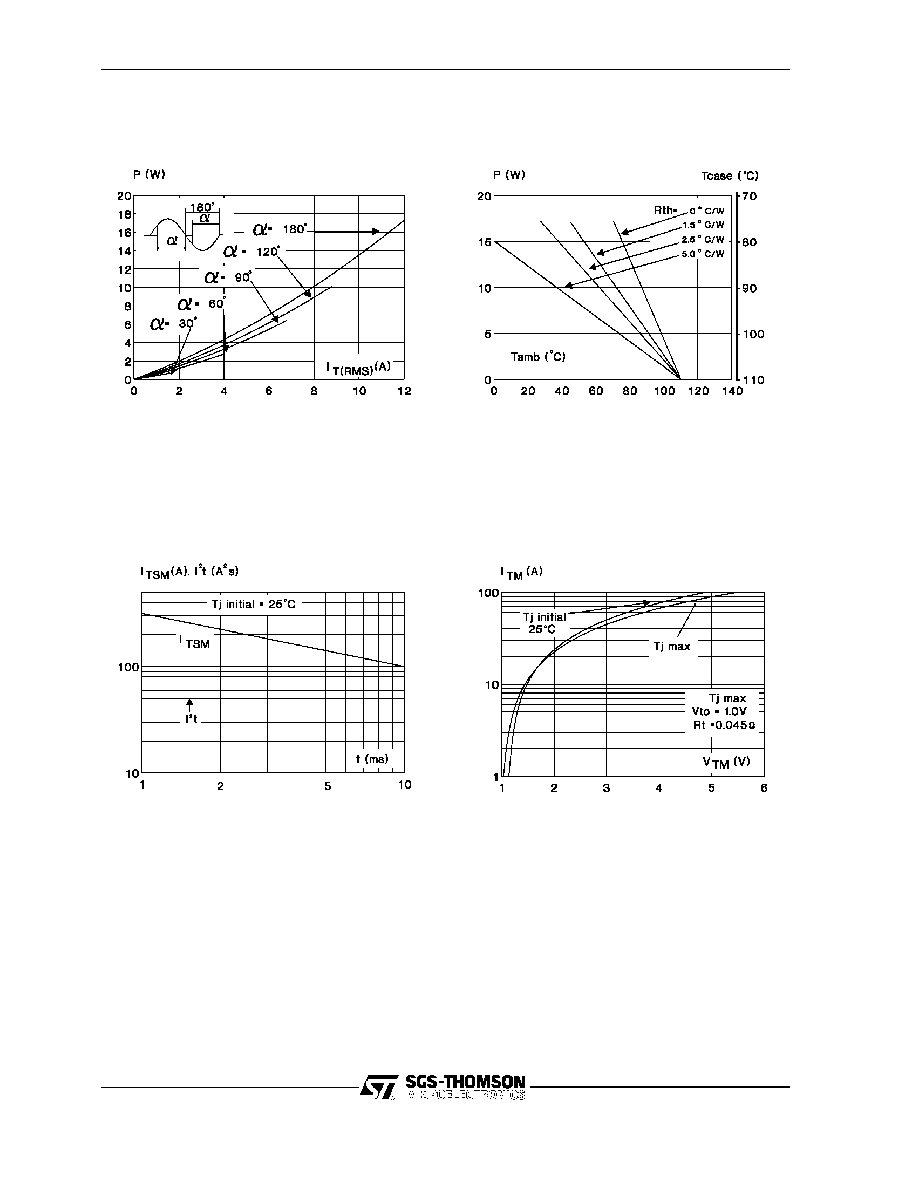
Fig. 1 :Maximum RMS power dissipation versus RMS on-
state current
(F = 60Hz).
(Curves are cut off by (dI/dt)c limitation)
Fig. 2 :Correlation between maximum mean power dissipa-
tion and maximum allowable temperatures (Tamb and
Tcase) for different thermal resistances heatsink + contact.
Fig. 3 :Non repetitive surge peak on state current for a
sinusoidal pulse with width : t
10ms, and corresponding
value of I2t.
Fig. 4 :On-state characteristics (maximum values).
AVS12
4/8

Symbo l
Parameter
Value
Unit
Min
T yp
Max
VSS (pin 1) (Vreg)
Shunt regulator
- 10
- 9
- 8
V
ISS (pin 1) (Vreg)
(@ VSS = 9V)
Supply current
0.4
30
mA
ISS (pin 1)
(@ triac gate non
connected)
Quiescent current
0.7
mA
f (pin 3)
(@ R = 91k
)
(C = 100pF)
Oscillator frequency
42
44
46
kHz
VM (pin 8) Vth (3)
Peak voltage of detection high-threshold
4.08
4.25
4.42
V
VM (pin 8) Vh (3)
Peak voltage of detection hysteresis
0.370
0.4
0.420
V
(1) VM (pin 8) Vth (3)
Zero-crossing detection high-threshold
95
110
125
mV
VM (pin 8) Vh (3)
Zero-crossing detection hysteresis
27
50
80
mV
(2)
Vrazht (4)
Power-on-reset activation threshold
Vreg x 0.89
V
(2)
Vrazlt (4)
Power-down-reset activation threshold
3
6.5
V
Mode (pin 7)
VIL
(4)
VIH
(4)
0.7 Vreg
0.3 Vreg
V
VG (pin 5)
VOL (IVG = 25mA)
Leakage current (VG = VDD)
650
+ 10
mV
µ
A
DC GENERAL ELECTRICAL CHARACTERISTICS (continued)
CONTROLLER AVS1ACP08 T
oper
= 25
∞
C (unless otherwise specified)
NOTES :
(1) : This value gives a typical noise immunity on the zero-crossing detection of 110mV x 1018/18 = 6.20V on the main supply
(2) : See following diagram
(3) : Voltage referred to VSS
(4) : Voltage referred to VDD
POWER-ON AND POWER-OFF RESET BEHAVIOUR
0V
0V
-2.7V
-2.7V
Vrazht
Vrazlt
Vreg = V
- V
SS
DD
Normal operation
Power-on
reset
Un determined
Undetermined
Reset
power-off
AVS12
5/8