 | –≠–ª–µ–∫—Ç—Ä–æ–Ω–Ω—ã–π –∫–æ–º–ø–æ–Ω–µ–Ω—Ç: B270N04 | –°–∫–∞—á–∞—Ç—å:  PDF PDF  ZIP ZIP |

February 2006
Rev3
1/14
14
100% avalanche tested
Standard threshold drive
Description
This N-Channel enhancement mode MOSFET is
the latest refinement of STMicroelectronic unique
"Single Feature SizeTM" strip-based process with
less critical aligment steps and therefore a
remarkable manufacturing reproducibility. The
resulting transistor shows extremely high packing
density for low on-resistance, rugged avalanche
characteristics and low gate charge.
Applications
High current, switching application
Automotive
Internal schematic diagram
General features
Type
V
DSS
R
DS(on)
I
D
P
TOT
STB270N04-1
40V
<2.9m
120A
330W
STB270N04
40V
<2.5m
160A
330W
STP270N04
40V
<2.9m
120A
330W
1
2
3
1
2
3
1
3
TO-220
D≤PAK
I≤PAK
STB270N04
STB270N04-1 - STP270N04
N-CHANNEL 40V - 2.1m
- 160A - TO-220 - D
2
PAK - I
2
PAK
STripFETTM Power MOSFET
www.st.com
Order codes
Sales Type
Marking
Package
Packaging
STB270N04-1
B270N04
I≤PAK
TUBE
STB270N04
B270N04
D≤PAK
TAPE & REEL
STP270N04
P270N04
TO-220
TUBE
Electrical ratings
STB270N04-1 - STB270N04 - STP270N04
2/14
Rev3
1 Electrical
ratings
Table 1.
Absolute maximum ratings
Symbol
Parameter
Value
Unit
TO-220/I≤PAK
D≤PAK
V
DS
Drain-Source Voltage (V
GS
= 0)
40
V
V
GS
Gate-Source Voltage
± 20
V
I
D
(1)
1.
Current limited by package
Drain Current (continuous) at T
C
= 25∞C
120
160
A
I
D
(1)
Drain Current (continuous) at T
C
=100∞C
120
160
A
I
DM
(2)
2.
Pulse width limited by safe operating area
Drain Current (pulsed)
480
640
A
P
TOT
Total Dissipation at T
C
= 25∞C
330
W
Derating Factor
2.2
W/∞C
dv/dt
(3)
3.
I
SD
120A, di/dt
200A/µs, V
DD
V
(BR)DSS
, T
j
T
JMAX
Peak Diode Recovery voltage slope 3.5 V/ns
E
AS
(4)
4.
Starting Tj=25∞C, Id =80A, Vdd=32V
Single Pulse Avalanche Energy
1
J
T
J
T
stg
Operating Junction Temperature
Storage Temperature
-55 to 175
∞C
Table 2.
Thermal data
Symbol
Parameter
Value
Unit
TO-220/I≤PAK
D≤PAK
R
thj-case
Thermal resistance junction-case Max
0.45
∞C/W
R
thj-pcb
(1)
1.
When mounted on 1inch≤ FR-4 board, 2 oz Cu.
Thermal resistance Junction-pcb Max
--
35
∞C/W
R
thj-a
Thermal resistance junction-ambient Max
62.5
--
∞C/W
T
l
Maximum lead temperature for soldering
purpose (for 10 sec, 1.6mm from case)
300
--
∞C
STB270N04-1 - STB270N04 - STP270N04
Electrical characteristics
Rev3
3/14
2 Electrical
characteristics
(T
CASE
=25∞C unless otherwise specified)
Table 3.
On/off states
Symbol
Parameter
Test Condictions
Min.
Typ.
Max.
Unit
V
(BR)DSS
Drain-Source
Breakdown Voltage
I
D
= 250
µ
A, V
GS
= 0
40
V
I
DSS
Zero Gate Voltage Drain
Current (V
GS
= 0)
V
DS
= Max Rating,
V
DS
= MaxRating
@125∞C
10
100
µA
µA
I
GSS
Gate Body Leakage
Current
(V
DS
= 0)
V
GS
= ±20V
±
200
nA
V
GS(th)
Gate Threshold Voltage
V
DS
= V
GS
, I
D
= 250µA
2
4
V
R
DS(on)
Static Drain-Source On
Resistance
V
GS
= 10V, I
D
= 80A
TO-220
I≤PAK
2.5
2.9
m
D≤PAK
2.1
2.5
m
Table 4.
Dynamic
Symbol
Parameter
Test Condictions
Min.
Typ.
Max.
Unit
g
fs
(1)
1.
Pulsed: pulse duration=300µs, duty cycle 1.5%
Forward Transconductance
V
DS
=15V, I
D
= 80A
200
S
C
iss
C
oss
C
rss
Input Capacitance
Output Capacitance
Reverse Transfer
Capacitance
V
DS
=25V, f=1 MHz, V
GS
=0
7400
1800
47
pF
pF
pF
Q
g
Q
gs
Q
gd
Total Gate Charge
Gate-Source Charge
Gate-Drain Charge
V
DD
=20V, I
D
= 160A
V
GS
=10V
(see Figure 2)
110
27
25
150
nC
nC
nC

Electrical characteristics
STB270N04-1 - STB270N04 - STP270N04
4/14
Rev3
Table 5.
Switching times
Symbol
Parameter
Test Condictions
Min.
Typ.
Max.
Unit
t
d(on)
t
r
Turn-on Delay Time
Rise Time
V
DD
=20 V, I
D
= 80A,
R
G
=4.7
,
V
GS
=10V
(see Figure 14)
22
180
ns
ns
t
d(off)
t
f
Turn-off Delay Time
Fall Time
V
DD
=20 V, I
D
= 80A,
R
G
=4.7
,
V
GS
=10V
(see Figure 14)
110
45
ns
ns
Table 6.
Source drain diode
Symbol
Parameter
Test Condictions
Min
Typ.
Max
Unit
I
SD
Source-drain Current
D≤PAK
160
A
TO-220
I≤PAK
120
A
I
SDM
(1)
1.
Pulse width limited by safe operating area
Source-drain Current
(pulsed)
D≤PAK
640
A
TO-220
I≤PAK
480
A
V
SD
(2)
2.
Pulsed: pulse duration=300µs, duty cycle 1.5%
Forward on Voltage
I
SD
=80A, V
GS
=0
1.5
V
t
rr
Q
rr
I
RRM
Reverse Recovery Time
Reverse Recovery Charge
Reverse Recovery Current
I
SD
=160A,
di/dt = 100A/µs,
V
DD
=32V, Tj=150∞C
70
225
3.2
ns
nC
A
STB270N04-1 - STB270N04 - STP270N04
Electrical characteristics
Rev3
5/14
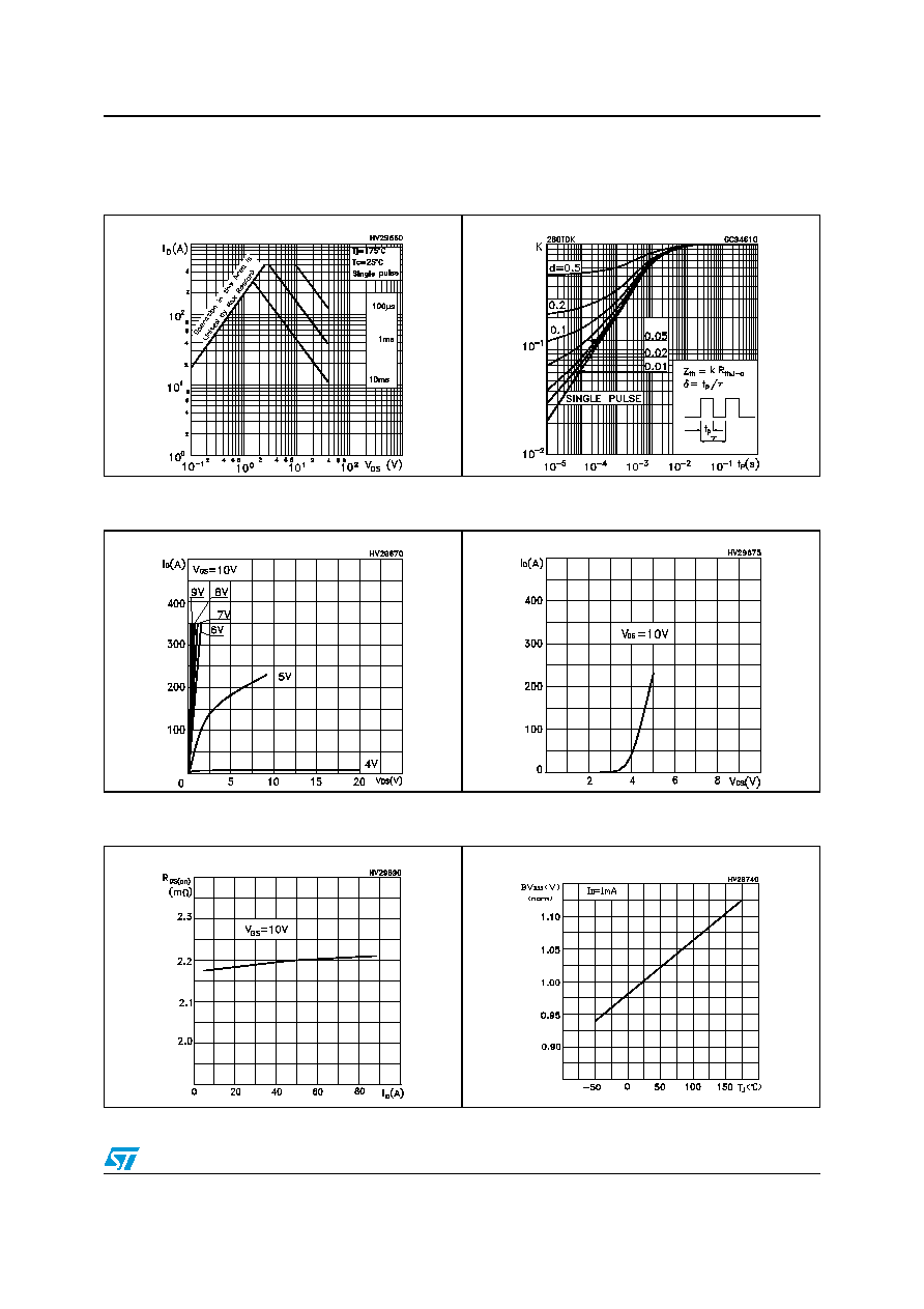
2.1
Electrical characteristics (curves)
Figure 1.
Safe operating area
Figure 2.
Thermal impedance
Figure 3.
Output characterisics
Figure 4.
Transfer characteristics
Figure 5.
Static drain-source on resistance
Figure 6.
Normalized B
VDSS
vs temperature

Electrical characteristics
STB270N04-1 - STB270N04 - STP270N04
6/14
Rev3
Figure 7.
Gate charge vs gate-source voltage Figure 8.
Capacitance variations
Figure 9.
Normalized gate threshold voltage
vs temperature
Figure 10. Normalized on resistance vs
temperature
Figure 11. Source-drain diode forward
characteristics
STB270N04-1 - STB270N04 - STP270N04
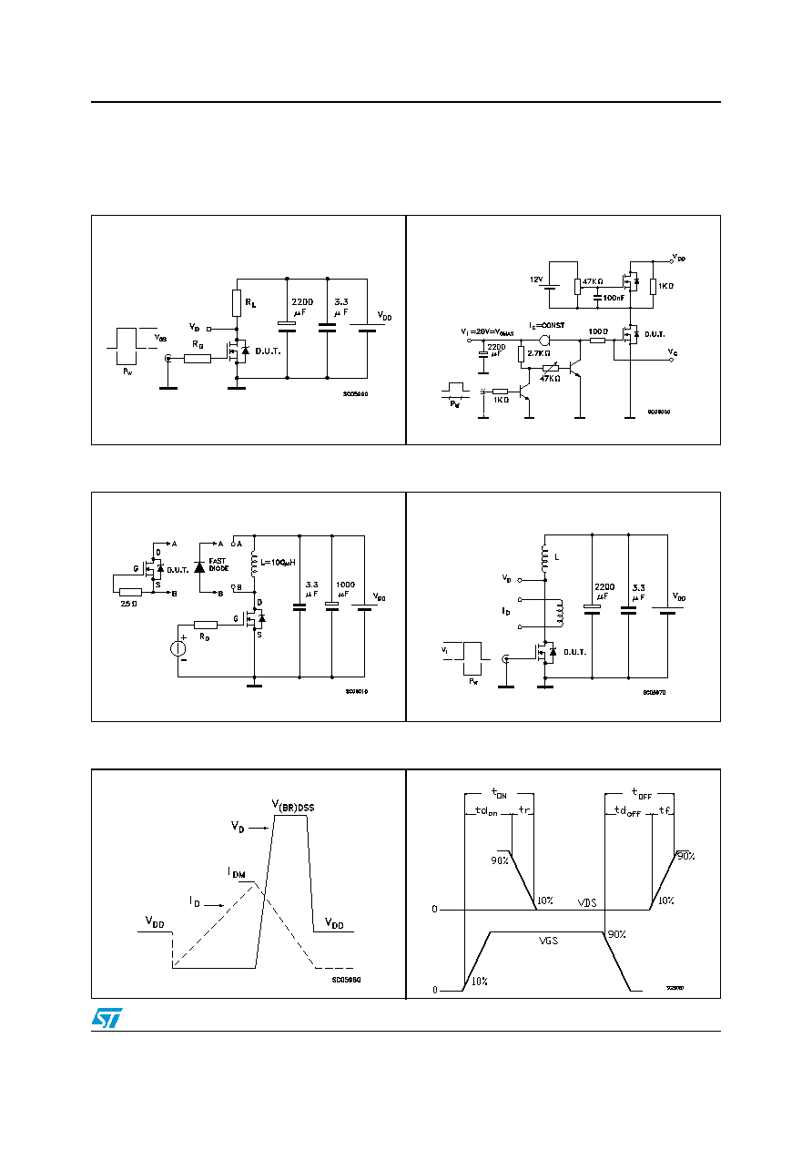
Test circuit
Rev3
7/14
3 Test
circuit
Figure 12. Switching times test circuit for
resistive load
Figure 13. Gate charge test circuit
Figure 14. Test circuit for inductive load
switching and diode recovery times
Figure 15. Unclamped Inductive load test
circuit
Figure 16. Unclamped inductive waveform
Figure 17. Switching time waveform

Package mechanical data
STB270N04-1 - STB270N04 - STP270N04
8/14
Rev3
4 Package
mechanical
data
In order to meet environmental requirements, ST offers these devices in ECOPACKÆ
packages. These packages have a Lead-free second level interconnect . The category of
second level interconnect is marked on the package and on the inner box label, in
compliance with JEDEC Standard JESD97. The maximum ratings related to soldering
conditions are also marked on the inner box label. ECOPACK is an ST trademark.
ECOPACK specifications are available at:
www.st.com

STB270N04-1 - STB270N04 - STP270N04
Package mechanical data
Rev3
9/14
DIM.
mm.
inch
MIN.
TYP
MAX.
MIN.
TYP.
MAX.
A
4.40
4.60
0.173
0.181
b
0.61
0.88
0.024
0.034
b1
1.15
1.70
0.045
0.066
c
0.49
0.70
0.019
0.027
D
15.25
15.75
0.60
0.620
E
10
10.40
0.393
0.409
e
2.40
2.70
0.094
0.106
e1
4.95
5.15
0.194
0.202
F
1.23
1.32
0.048
0.052
H1
6.20
6.60
0.244
0.256
J1
2.40
2.72
0.094
0.107
L
13
14
0.511
0.551
L1
3.50
3.93
0.137
0.154
L20
16.40
0.645
L30
28.90
1.137
¯P
3.75
3.85
0.147
0.151
Q
2.65
2.95
0.104
0.116
TO-220 MECHANICAL DATA

Package mechanical data
STB270N04-1 - STB270N04 - STP270N04
10/14
Rev3
DIM.
mm.
inch
MIN.
TYP
MAX.
MIN.
TYP.
MAX.
A
4.40
4.60
0.173
0.181
A1
2.40
2.72
0.094
0.107
b
0.61
0.88
0.024
0.034
b1
1.14
1.70
0.044
0.066
c
0.49
0.70
0.019
0.027
c2
1.23
1.32
0.048
0.052
D
8.95
9.35
0.352
0.368
e
2.40
2.70
0.094
0.106
e1
4.95
5.15
0.194
0.202
E
10
10.40
0.393
0.410
L
13
14
0.511
0.551
L1
3.50
3.93
0.137
0.154
L2
1.27
1.40
0.050
0.055
TO-262 (I
2
PAK) MECHANICAL DATA
STB270N04-1 - STB270N04 - STP270N04
Package mechanical data
Rev3
11/14
TO-247 MECHANICAL DATA
1
DIM.
mm.
inch
MIN.
TYP
MAX.
MIN.
TYP.
MAX.
A
4.4
4.6
0.173
0.181
A1
2.49
2.69
0.098
0.106
A2
0.03
0.23
0.001
0.009
B
0.7
0.93
0.027
0.036
B2
1.14
1.7
0.044
0.067
C
0.45
0.6
0.017
0.023
C2
1.23
1.36
0.048
0.053
D
8.95
9.35
0.352
0.368
D1
8
0.315
E
10
10.4
0.393
E1
8.5
0.334
G
4.88
5.28
0.192
0.208
L
15
15.85
0.590
0.625
L2
1.27
1.4
0.050
0.055
L3
1.4
1.75
0.055
0.068
M
2.4
3.2
0.094
0.126
R
0.4
0.015
V2
0∫
4∫
D
2
PAK MECHANICAL DATA
3
Packaging mechanical data
STB270N04-1 - STB270N04 - STP270N04
12/14
Rev3
5 Packaging
mechanical
data
TAPE AND REEL SHIPMENT
D
2
PAK FOOTPRINT
* on sales type
DIM.
mm
inch
MIN.
MAX.
MIN.
MAX.
A
330
12.992
B
1.5
0.059
C
12.8
13.2
0.504
0.520
D
20.2
0795
G
24.4
26.4
0.960
1.039
N
100
3.937
T
30.4
1.197
BASE QTY
BULK QTY
1000
1000
REEL MECHANICAL DATA
DIM.
mm
inch
MIN.
MAX.
MIN.
MAX.
A0
10.5
10.7
0.413
0.421
B0
15.7
15.9
0.618
0.626
D
1.5
1.6
0.059
0.063
D1
1.59
1.61
0.062
0.063
E
1.65
1.85
0.065
0.073
F
11.4
11.6
0.449
0.456
K0
4.8
5.0
0.189
0.197
P0
3.9
4.1
0.153
0.161
P1
11.9
12.1
0.468
0.476
P2
1.9
2.1
0.075
0.082
R
50
1.574
T
0.25
0.35
0.0098 0.0137
W
23.7
24.3
0.933
0.956
TAPE MECHANICAL DATA

STB270N04-1 - STB270N04 - STP270N04
Revision history
Rev3
13/14
6 Revision
history
Table 7.
Document revision history
Date
Revision
Changes
07-Oct-2005
1
Initial release.
10-Nov-2005
2
Preliminary version
09-Feb-2006
3
Complete datasheet

STB270N04-1 - STB270N04 - STP270N04
14/14
Rev3
Information furnished is believed to be accurate and reliable. However, STMicroelectronics assumes no responsibility for the consequences
of use of such information nor for any infringement of patents or other rights of third parties which may result from its use. No license is granted
by implication or otherwise under any patent or patent rights of STMicroelectronics. Specifications mentioned in this publication are subject
to change without notice. This publication supersedes and replaces all information previously supplied. STMicroelectronics products are not
authorized for use as critical components in life support devices or systems without express written approval of STMicroelectronics.
The ST logo is a registered trademark of STMicroelectronics.
All other names are the property of their respective owners
© 2006 STMicroelectronics - All rights reserved
STMicroelectronics group of companies
Australia - Belgium - Brazil - Canada - China - Czech Republic - Finland - France - Germany - Hong Kong - India - Israel - Italy - Japan -
Malaysia - Malta - Morocco - Singapore - Spain - Sweden - Switzerland - United Kingdom - United States of America
www.st.com