 | –≠–ª–µ–∫—Ç—Ä–æ–Ω–Ω—ã–π –∫–æ–º–ø–æ–Ω–µ–Ω—Ç: B5S16861 | –°–∫–∞—á–∞—Ç—å:  PDF PDF  ZIP ZIP |
1/10
October 2004
s
HIGH SPEED: t
PD
= 0.25ns (MAX.)
at V
CC
= 4.5V T
A
=85∞C
s
ON RESISTANCE BETWEEN TWO PORT:
5
(TYP) at V
CC
= 5.0V T
A
=25∞C
s
LOW POWER DISSIPATION:
I
CC
= 1uA(MAX.) at T
A
=25∞C
s
COMPATIBLE WITH TTL OUTPUTS:
V
IH
=2V(MIN), V
IL
=0.8V(MAX)
s
POWER DOWN PROTECTION ON INPUTS
AND OUTPUTS
s
OPERATING VOLTAGE RANGE:
V
CC
(OPR) = 4V to 5.5V
s
PIN AND FUNCTION COMPATIBLE WITH
74 SERIES 16861
s
IMPROVED LATCH-UP IMMUNITY
s
ESD PERFORMANCE:
HBM > 2000V (MIL STD 883 method 3015);
MM > 200V
DESCRIPTION
The B5S16861 is an advanced high-speed CMOS
20-BIT TWO PORT BUS SWITCH fabricated with
sub-micron silicon gate and double-layer metal
wiring C
2
MOS technology.
It is ideal for 4V to 5.5V V
CC
operations and
ultra-low power and low noise applications,
typically notebook and docking station.
Any nG output control governs two 10-bit BUS
SWITCHES. Output Enable inputs (nG) tied
together gives full 20-bit operations. When nG is
LOW, the switches are on. When nG is HIGH, the
switches are in high impedance state.
It has ultra high-speed performance at 5V near
zero delay with low ON resistance.
All inputs and outputs are equipped with
protection circuits against static discharge, giving
them 2KV ESD immunity and transient excess
voltage.
B5S16861
20-BIT TWO PORT BUS SWITCH
This is preliminary information on a new product now in development are or undergoing evaluation. Details subject to change without notice.
Table 1: Order Codes
PACKAGE
T & R
TSSOP48
B5S16861TTR
TSSOP
PRELIMINARY DATA
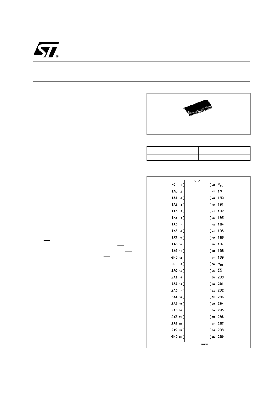
Figure 1: Pin Connection
Rev. 1

B5S16861
2/10
Figure 2: Input Equivalent Circuit
Table 2: Pin Description
Table 3: Truth Table
n: 0 to 9
X: "H" or "L"
Z: High Impedance
Figure 3: Schematic Diagram
PIN N∞
SYMBOL
NAME QND FUNCTION
1, 13
NC
Not Connected
2, 3, 4, 5, 6, 7,
8, 9, 10, 11
1A0 to 1A9 Data Inputs
14, 15, 16, 17,
18, 19, 20, 21,
22, 23
2A0 to 2A9 Data Inputs
34, 33, 32, 31,
30, 29, 28, 27,
26, 25
2B0 to 2B9 Data Outputs
46, 45, 44, 43,
42, 41, 40, 39,
38, 37
1B0 to 1B9 Data Outputs
47, 35
1G, 2G
Bus Enable Input
(Active Low)
12, 24
GND
Ground (0V)
36, 48
V
CC
Positive Supply Voltage
INPUT
OUTPUT
nG
1An, 2An
1Bn, 2Bn
L
X
Bus ON
H
X
Z
B5S16861
3/10
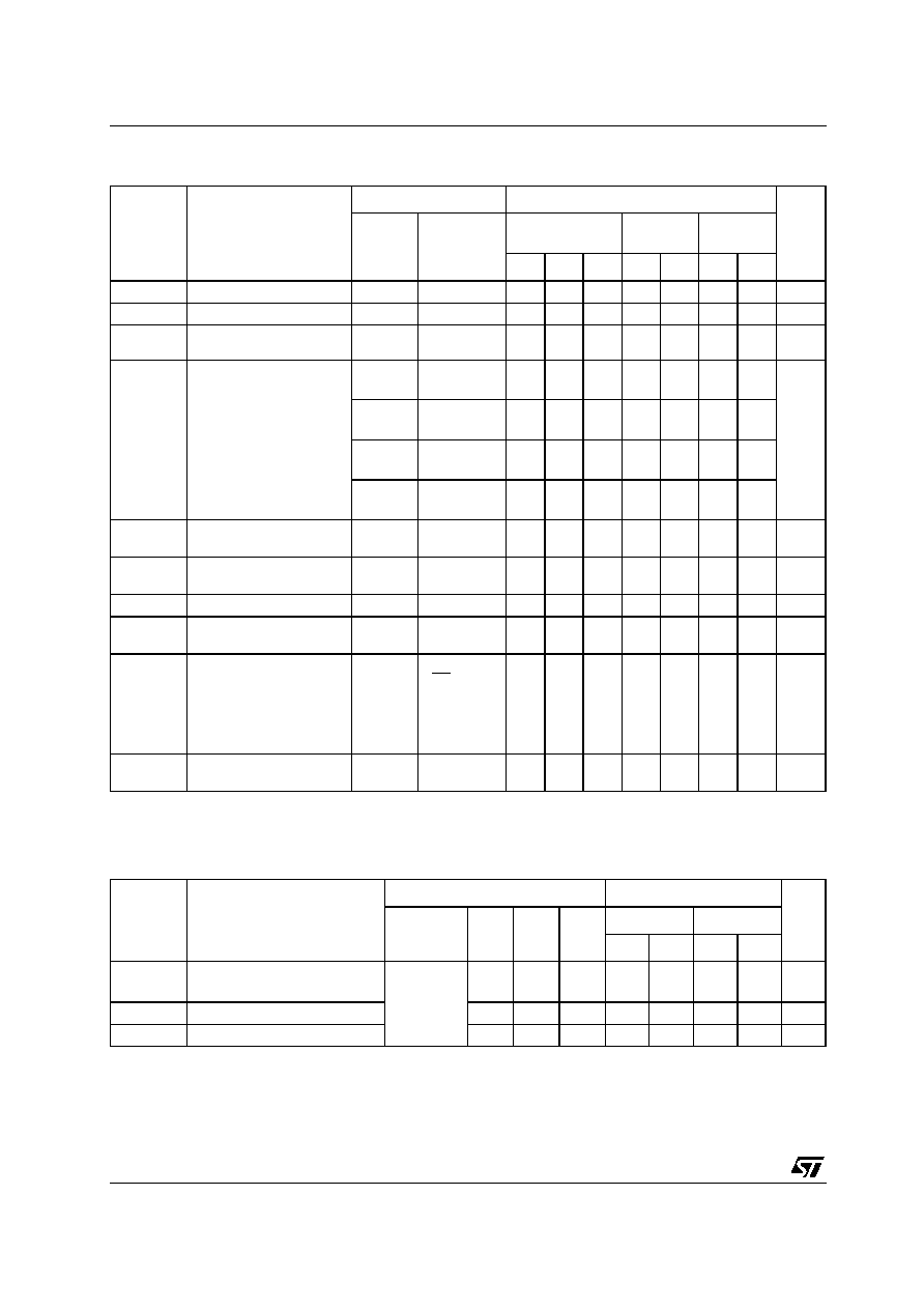
Table 4: Absolute Maximum Ratings
Absolute Maximum Rating are those value beyond which damage to the device may occur. Functional operation under these condition is not
implied
1) I
O
absolute maximum rating must be observed
2) V
O
< GND
3) Not more than one output should be tested at one time. Duration of the test should not exceed one second.
Table 5: Recommended Operating Conditions
1) V
IN
from 0.8V to 2V at V
CC
= 3.0V
Symbol
Parameter
Value
Unit
V
CC
Supply Voltage
-0.5 to +7.0
V
V
I
DC Switch and Control Pin Voltage
-0.5 to +7.0
V
V
O
DC Output Voltage (V
CC
= 0V) (note 1)
-0.5 to +7.0
V
V
O
DC Output Voltage (V
I/O
=Gnd)
-0.5 to +7.0
V
I
IK
DC Input Diode Current (V
I/O
< 0V)
- 50
mA
I
OK
DC Output Diode Current (note 2)
- 50
mA
I
O
DC Output Current (note 3)
128
mA
I
CC
or I
GND
DC V
CC
or Ground Current per Supply Pin
±
100
mA
T
stg
Storage Temperature
-65 to +150
∞C
T
L
Lead Temperature (10 sec)
300
∞C
Symbol
Parameter
Value
Unit
V
CC
Supply Voltage
4 to 5.5
V
V
I
Input Voltage
0 to 5.5
V
V
O
Output Voltage (V
CC
= 0V)
0 to 5.5
V
V
O
Output Voltage
0 to 5.5
V
T
op
Operating Temperature
-55 to 125
∞C
dt/dv
Switch Input Rise and Fall Time
0 to DC
ns/V
dt/dv
Control Input Rise and Fall Time (note 1)
0 to 10
ns/V
B5S16861
4/10
Table 6: DC Specification
1) This current applies to the control inputs only and represent the current required to switch internal capacitance at the specified frequency.
The 1An and 2An inputs generate no significant AC or DC currents as they transition. This parameter is not tested, but is guaranteed by
design.
Table 7: AC Electrical Characteristics
1) Parameter guaranteed by design
2) X=1,2; n=0..9.
Symbol
Parameter
Test Condition
Value
Unit
V
CC
(V)
T
A
= 25 ∞C
-40 to 85
∞C
-55 to 125
∞C
Min. Typ. Max. Min. Max. Min. Max.
V
IH
High Level Input Voltage
4 to 5.5
2
2
2
V
V
IL
Low Level Input Voltage
4 to 5.5
0.8
0.8
0.8
V
V
H
Input Hysteresis at
Control pin
4.5 to 5.5
150
mV
R
ON
Switch ON Resistance
4.5
I
ON
=64 mA
V
I
=0V
7
4.5
I
ON
=48 mA
V
I
=0V
5
7
4.5
I
ON
=15 mA
V
I
=2.4V
10
15
4.0
I
ON
=15 mA
V
I
=2.4V
14
22
I
I
Input Leakage Current
0 to 5.5
V
I
= 5.5V or
GND
±
0.1
±
1.0
±
2.0
µ
A
I
OZ
High Impedance Leakage
Current
4.5 to 5.5
V
I/O
= 5.5V
to GND
±
1.0
±
2.0
µ
A
V
IK
Clamp Diode Voltage
4.0 to 5.5
I
I
= -18mA
-0.7
-1.2
-1.2
V
I
CC
Quiescent Supply Current
5.5
V
I
= V
CC
or
GND
0.1
1.0
3.0
10.0
µ
A
I
CCD
Supply Current per
Control Input per MHz (1)
5.5
V
I/O
= Open
nG=GND;
Control Input
Toggling
50% Duty
Cycle
0.25
mA/
MHz
I
CC
I
CC
incr. per Input
5.5
V
IC
=V
CC
-2.1
V
2.5
mA
Symbol
Parameter
Test Condition
Value
Unit
V
CC
(V)
C
L
(pF)
R
L
(
)
t
s
= t
r
(ns)
-40 to 85 ∞C -55 to 125∞C
Min.
Max.
Min.
Max.
t
PLH
t
PHL
Propagation Delay Time (1)
xAn to xBn, xBn to xAn(2)
4.5 to 5.5
50
500
2.5
0.25
ns
t
PZL
t
PZH
Output Enable Time
50
500
2.5
1.5 5.5
ns
t
PLZ
t
PHZ
Output Disable Time
50
500
2.5
1.5 5.5
ns
B5S16861
5/10
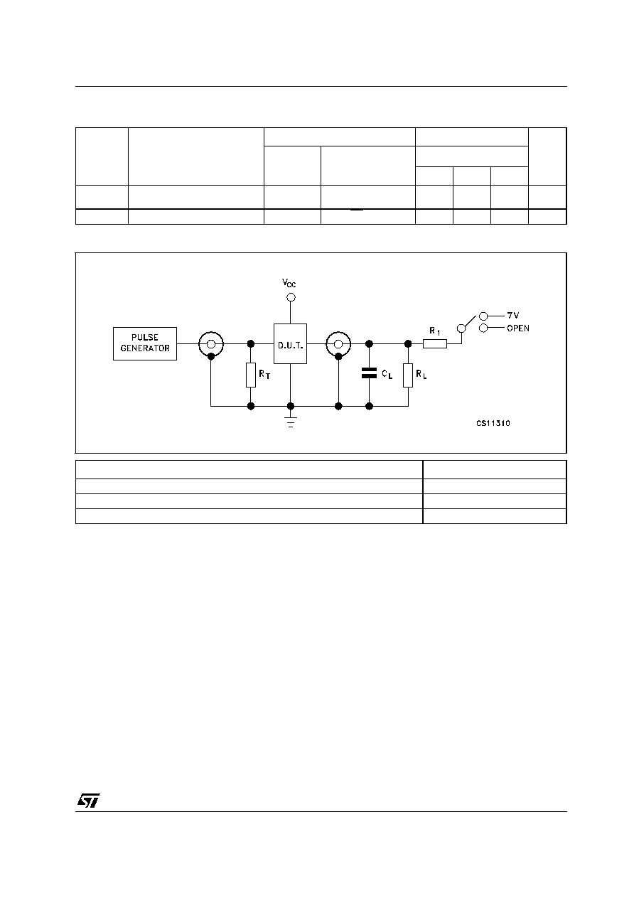
Table 8: Capacitance Characteristics
Figure 4: Test Circuit
C
L
= 50pF or equivalent (includes jig and probe capacitance)
R
L
= R
1
= 500
or equivalent
R
T
= Z
OUT
of pulse generator (typically 50
)
Symbol
Parameter
Test Condition
Value
Unit
V
CC
(V)
T
A
= 25 ∞C
Min.
Typ.
Max.
C
IN
Input Capacitance at Control
Pin
4
pF
C
I/O
Input Capacitance at I/O Pin
5.0
nG=V
CC
5.5
pF
TEST
SWITCH
t
PLH
, t
PHL
Open
t
PZL
, t
PLZ
7V
t
PZH
, t
PHZ
Open