 | –≠–ª–µ–∫—Ç—Ä–æ–Ω–Ω—ã–π –∫–æ–º–ø–æ–Ω–µ–Ω—Ç: BAR63J | –°–∫–∞—á–∞—Ç—å:  PDF PDF  ZIP ZIP |

1/4
BAR63J
Æ
April 2003 - Ed: 2B
PIN DIODE
n
Pin diode for high speed switching of RF signal
n
Low forward voltage
n
Very low capacitance
FEATURES AND BENEFITS
Single pin diode in SOD-323 package. This diode
is intended to be used in mobile phone to switch
the RF signal.
DESCRIPTION
SOD-323
Symbol
Parameter
Value
Unit
V
R
Continuous reverse voltage
50
V
I
F
Continuous forward current
100
mA
P
tot
Power Dissipation
T
s
< 55∞C
250
mW
T
stg
Storage temperature range
- 65 to +150
∞C
Tj
Maximum junction temperature
150
∞C
TL
Maximum temperature for soldering
260
∞
C
ABSOLUTE RATINGS (limiting values)
A
K
35
Symbol
Parameter
Value
Unit
R
th (j-a)
Junction to ambient (see note 1)
550
∞C/W
Note 1: Epoxy board with recommended pad layout.
THERMAL RESISTANCE
BAR63J
2/4
Symbol
Parameter
Tests Conditions
Min.
Typ.
Max. Unit
V
F
Forward voltage drop
T
amb
= 25∞C
I
F
= 100 mA
0.95
1.2
V
I
R
Continuous reverse current
T
amb
= 25∞C
V
R
= 50 V
50
nA
V
BR
Reverse avalanche breakdown
voltage
I
R
= 5 µA
50
V
STATIC ELECTRICAL CHARACTERISTICS
Symbol
Parameter
Tests Conditions
Min.
Typ.
Max.
Unit
C
t
Diode capacitance
V
R
= 0 V
F = 1 MHz
0.4
pF
V
R
= 5 V
F = 1 MHz
0.21
0.3
r
f
Forward resistance
I
F
= 5 mA
F = 100 MHz
1.8
2
Ohm
L
s
Series inductance
1.8
nH
t
rr
Charge carrier life time
I
F
= 10 mA
I
R
= 10 mA
I
R
= 6 mA
125
nS
ELECTRICAL CHARACTERISTICS
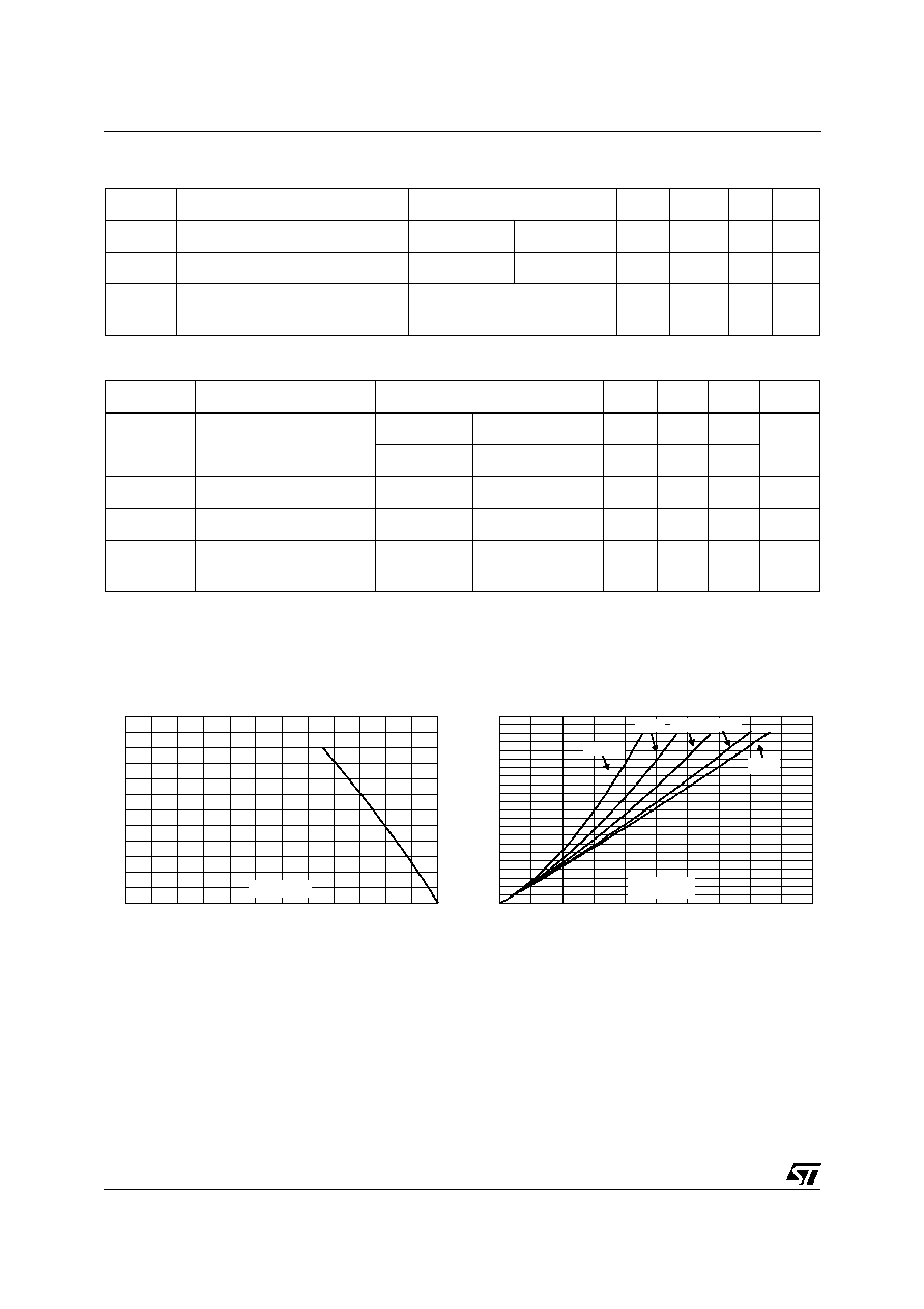
0
20
40
60
80
100
120
0
25
50
75
100
125
150
I (mA)
F
T
(∞C)
amb
Fig. 1: Forward current versus ambient tempera-
ture (epoxy board with recommended pad layout).
0
10
20
30
40
50
60
70
80
90
100
110
0
25
50
75
100
125
P
(mW)
F(AV)
I
(mA)
F(AV)
= 0.5
= 0.05
= 0.1
= 0.2
= 1
Fig. 2: Average forward power dissipation versus
average forward current.

BAS70-07
3/4
0
50
100
150
200
250
300
350
400
450
500
0
5
10
15
20
25
30
C(fF)
V (V)
R
F=1MHz
V
=30mV
T =25∞C
OSC
RMS
j
Fig. 3: Junction capacitance versus reverse
voltage applied (typical values).
0.1
1.0
10.0
0.1
1.0
10.0
100.0
R (W)
F
I (mA)
F
F=100MHz
T =25∞C
j
Fig. 4: Forward resistance versus forward current
(typical values).
300
350
400
450
500
550
600
0
5
10
15
20
25
30
35
40
45
50
S(mm≤)
R
(∞C/W)
th(j-a)
Fig. 5: Thermal resistance junction to ambient ver-
sus copper surface under each lead (printed circuit
board, epoxy FR4, Cu=35µm).
100.000k
1.500G
3.000G
4.500G
6.000G
- 30.00
- 22.50
- 15.00
- 7.50
0.00
Aplac
7.62 User: ST Microelectronics May 31 2002
f/Hz
14.39
isolation dB
0.66
insertion losses
dB
SOD package
@900MHz
14.39
isolation dB
0.66
insertion losses
dB
SOD package
@900MHz
SOD 323 0v
SOD 323 2.7v
Fig. 6: Insertion losses from antenna to receiver at
V
BIAS
= 0V and 2.7V.
100.000k
1.500G
3.000G
4.500G
6.000G
- 30.00
- 22.50
- 15.00
- 7.50
0.00
Aplac
7.62 User: ST Microelectronics May 31 2002
f/Hz
14.97
isolation dB
Vbias 2.7v
19.84
isolation dB
Vbias 0v
SOD package
@900MHz
14.97
isolation dB
Vbias 2.7v
19.84
isolation dB
Vbias 0v
SOD package
@900MHz
SOD 323 0v
SOD 323 2.7v
Fig. 7: Insertion losses from transceiver to re-
ceiver at V
BIAS
= 0V and 2.7V.
100.000k
1.500G
3.000G
4.500G
6.000G
- 30.00
- 22.50
- 15.00
- 7.50
0.00
Aplac
7.62 User: ST Microelectronics May 31 2002
f/Hz
19.35
isolation dB
0.88
insertion losses
dB
SOD package
@900MHz
19.35
isolation dB
0.88
insertion losses
dB
SOD package
@900MHz
SOD 323 0v
SOD 323 2.7v
Fig. 8: Insertion losses from transceiver to an-
tenna at V
BIAS
= 0V and 2.7V.
BAR63J
4/4
Information furnished is believed to be accurate and reliable. However, STMicroelectronics assumes no responsibility for the consequences of
use of such information nor for any infringement of patents or other rights of third parties which may result from its use. No license is granted by
implication or otherwise under any patent or patent rights of STMicroelectronics. Specifications mentioned in this publication are subject to
change without notice. This publication supersedes and replaces all information previously supplied.
STMicroelectronics products are not authorized for use as critical components in life support devices or systems without express written
approval of STMicroelectronics.
The ST logo is a registered trademark of STMicroelectronics
© 2003 STMicroelectronics - Printed in Italy - All rights reserved.
STMicroelectronics GROUP OF COMPANIES
Australia - Brazil - Canada - China - Finland - France - Germany
Hong Kong - India - Israel - Italy - Japan - Malaysia - Malta - Morocco - Singapore
Spain - Sweden - Switzerland - United Kingdom - United States.
http://www.st.com
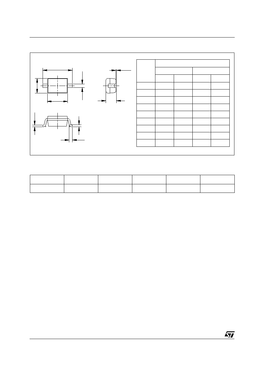
PACKAGE MECHANICAL DATA
SOD-323
H
b
D
E
A1
A
L
Q1
c
Type
Marking
Package
Weight
Base qty
Delivery mode
BAR63J
35
SOD-323
0.005g
3000
Tape & reel
MARKING
REF.
DIMENSIONS
Millimeters
Inches
Min.
Max.
Min.
Max.
A
1.17
0.046
A1
0
0.1
0
0.004
b
0.25
0.44
0.01
0.017
c
0.1
0.25
0.004
0.01
D
1.52
1.8
0.06
0.071
E
1.11
1.45
0.044
0.057
H
2.3
2.7
0.09
0.106
L
0.1
0.46
0.004
0.02
Q1
0.1
0.41
0.004
0.016