 | –≠–ª–µ–∫—Ç—Ä–æ–Ω–Ω—ã–π –∫–æ–º–ø–æ–Ω–µ–Ω—Ç: BAS69 | –°–∫–∞—á–∞—Ç—å:  PDF PDF  ZIP ZIP |

July 2006
Rev 1
1/9
BAS69 Series
Low capacitance small signal Schottky diodes
Main product characteristics
Features and benefits
Low diode capacitance
Designed for RF applications
Low profile packages
Very low parasitic inductor and resistor
Description
The BAS69 series use 15V barrier, with extremely
low junction capacitance, suitable for the
detection of an RF signal and the compensation
of the voltage drift with the temperature. The
presented packages make the device ideal in
applications where space saving is critical.
The low junction capacitance will reduce the
disturbance on the RF signal.
Order codes
I
F
10 mA
V
RRM
15 V
C
(typ)
<1 pF
T
j
(max)
150∞ C
Part Number
Marking
BAS69WFILM
23
BAS69-04WFILM
24
BAS69-05WFILM
25
BAS69-06WFILM
26
BAS69KFILM
65
BAS69-09P6FILM
69
BAS69-07P6FILM
67
SOD-523
SOT-666
BAS69KFILM
(Single)
BAS69WFILM
(Single)
BAS69-05WFILM
(Common cathode)
BAS69-06WFILM
(Common anode)
BAS69-04WFILM
(Series)
BAS69-07P6FILM
(2 parallel diodes)
BAS69-09P6FILM
(2 opposite diodes)
SOT-323
Configurations in top view
www.st.com

Characteristics
BAS69 Series
2/9
1 Characteristics
Table 1.
Absolute ratings (limiting values at T
j
= 25∞ C, unless otherwise specified)
Symbol
Parameter
Value
Unit
V
RRM
Repetitive peak reverse voltage
15
V
I
F
Continuous forward current
10
mA
I
FSM
Surge non repetitive forward current
Half wave, single phase 60 Hz
2
A
T
stg
Storage temperature range
-65 to +150
∞ C
T
j
Maximum operating junction temperature
(1)
150
T
L
Maximum soldering temperature
(1)
260
1.
Pulse test: t
p
= 380 µs,
< 2 %
Table 2.
Thermal parameters
Symbol
Parameter
Value
Unit
R
th(j-a)
Junction to ambient
(1)
SOT-323 550
∞ C/W
SOD-523, SOT-666
600
1.
Epoxy printed circuit board with recommended pad layout
Table 3.
Static electrical characteristics
Symbol
Parameter
Test conditions
Min.
Typ
Max.
Unit
I
R
(1)
Reverse leakage current
T
j
= 25∞ C
V
R
= 1 V
0.035
µA
T
j
= 125∞ C
6
30
T
j
= 25∞ C
V
R
= 15 V
0.23
T
j
= 125∞ C
10
100
V
F
(1)
Forward voltage drop
T
j
= 25∞ C
I
F
= 1 mA
350
380
mV
T
j
= 125∞ C
230
260
T
j
= 25∞ C
I
F
= 10 mA
500
570
T
j
= 125∞ C
460
510
1.
Pulse test: t
p
250 ms, 2 %
Table 4.
Dynamic characteristics
Symbol
Parameter
Test conditions
Min.
Typ
Max.
Unit
C
Diode capacitance
V
R
= 0 V, F = 1 MHz
1.0
pF
R
F
Forward resistance
I
F
= 5 mA, F = 100 MHz
15
L
S
Series inductance
1.5
nH

BAS69 Series
Characteristics
3/9
Figure 1.
Forward voltage drop versus
forward current (typical values)
Figure 2.
Reverse leakage current versus
reverse voltage applied (typical
values)
1.E-01
1.E+00
1.E+01
1.E+02
0.0
0.2
0.4
0.6
0.8
1.0
1.2
V
(V)
FM
Tj=125∞C
Tj=125∞C
Tj=85∞C
Tj=85∞C
Tj=25∞C
Tj=25∞C
Tj=-40∞C
Tj=-40∞C
I
(mA)
FM
1.E-03
1.E-02
1.E-01
1.E+00
1.E+01
1.E+02
0.0
2.5
5.0
7.5
10.0
12.5
15.0
V (V)
R
Tj=125∞C
Tj=85∞C
Tj=25∞C
I (µA)
R
Figure 3.
Differential forward resistance
versus forward current (typical
values)
Figure 4.
Junction capacitance versus
reverse voltage applied (typical
values)
1
10
100
1.0
10.0
100.0
I (mA)
F
F=10kHz
Tj=25∞C
R ( )
F
0.0
0.1
0.2
0.3
0.4
0.5
0.6
0.7
0.8
0.9
1.0
0.0
2.5
5.0
7.5
10.0
12.5
15.0
V (V)
R
F=1MHz
Vosc=30mV
RMS
Tj=25∞C
C(pF)
Figure 5.
Relative variation of thermal
impedance junction to ambient
versus pulse duration (SOT-323)
Figure 6.
Relative variation of thermal
impedance junction to ambient
versus pulse duration (SOT-666)
1.E-03
1.E-02
1.E-01
1.E+00
1.E-03
1.E-02
1.E-01
1.E+00
1.E+01
1.E+02
1.E+03
Single pulse
SOT-323
Epoxy FR4
S
CU
=2.25 mm≤
e
CU
=35 µm
(s)
t
P
Z
th(j-a)
/R
th(j-a)
1.E-02
1.E-01
1.E+00
1.E-03
1.E-02
1.E-01
1.E+00
1.E+01
Single pulse
SOT-666
Epoxy FR4
e
CU
=35 µm
(s)
t
P
Z
th(j-a)
/R
th(j-a)
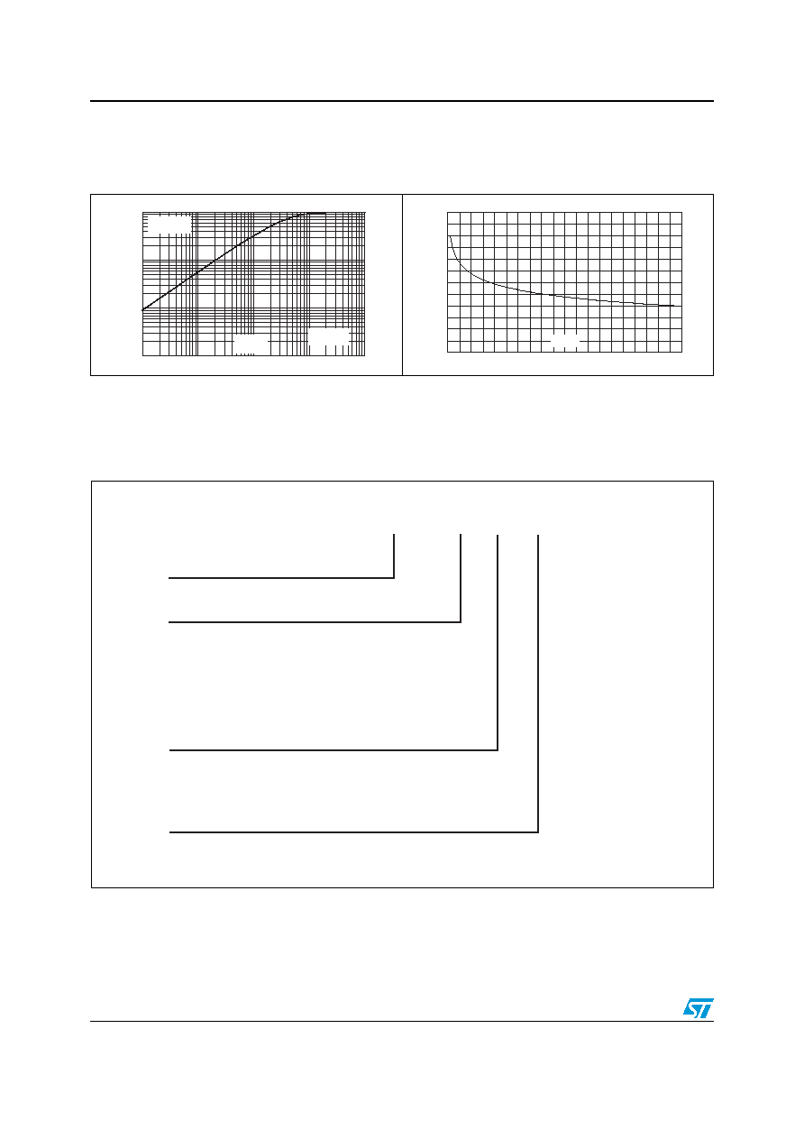
Ordering information scheme
BAS69 Series
4/9
2
Ordering information scheme
Figure 7.
Relative variation of thermal
impedance junction to ambient
versus pulse duration (SOD-523)
Figure 8.
Thermal resistance junction to
ambient versus copper surface
under each lead (printed circuit
board, epoxy FR4 - SOT-323)
1.E-03
1.E-02
1.E-01
1.E+00
1.E-03
1.E-02
1.E-01
1.E+00
1.E+01
Single pulse
SOD-523
Epoxy FR4
e
CU
=35 µm
Z
th(j-a)
/R
th(j-a)
(s)
t
P
300
350
400
450
500
550
600
0
5
10
15
20
25
30
35
40
45
50
S
(mm≤)
CU
R (j-a)
th
BAS69 xx xx FILM
Signal Schottky diodes
Package
V
= 15 V
RRM
No letter = Single diode
04 =
05 = Common cathode
06 =
07 = Parallel diodes
09 = Opposite diodes
Series diodes
Common anode
W = SOT-323
K = SOD-523
P6 = SOT-666
Configuration
Packing
FILM = Tape and reel

BAS69 Series
Package information
5/9
3 Package
information
Epoxy meets UL94, V0
Figure 9.
SOD-523 footprint (dimensions in mm)
Table 5.
SOD-523 dimensions
Ref.
Dimensions
Millimeters
Inches
Min.
Typ.
Max.
Min.
Typ.
Max.
A
0.50
0.60
0.70
0.020 0.024 0.028
E
1.50
1.60
1.70
0.059 0.063 0.067
E1
1.10
1.20
1.30
0.043 0.047 0.051
D
0.70
0.80
0.90
0.028 0.031 0.035
b
0.25
0.35
0.010
0.014
c
0.07
0.20
0.003
0.008
L
0.15
0.20
0.25
0.006 0.008 0.010
L1
0.10
0.20
0.004
0.008
E1
2xb
SEATING PLANE
R0.1
c
8∞
7∞
L
D
E
0.15
0.20
C
C
A
A
B
B
B
A
C
A
L1
M
M
0.7
0.3
2