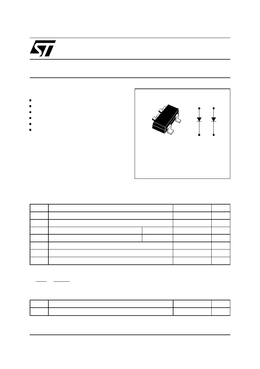
BAS70-07
Æ
June 1999 - Ed: 2A
SMALL SIGNAL SCHOTTKY DIODE
VERY SMALL CONDUCTION LOSSES
NEGLIGIBLE SWITCHING LOSSES
LOW FORWARD VOLTAGE DROP
LOW THERMAL RESISTANCE
EXTREMELY FAST SWITCHING
SURFACE MOUNTED DEVICE
FEATURES AND BENEFITS
Low turn-on and high breakdown voltage diodes
intended for
ultrafast switching and UHF detectors in hybrid mi-
cro circuits. Packaged in SOT-143, this device is
intended for surface mounting. Its dual inde-
pendent diodes configuration makes it very inter-
esting for applications where high integration is
searched.
DESCRIPTION
SOT-143
Symbol
Parameter
Value
Unit
V
RRM
Repetitive peak reverse voltage
70
V
I
F
Continuous forward current
15
mA
I
FSM
Surge non repetitive forward current
tp = 10ms
1
A
P
tot
Power Dissipation (note 1)
T
amb
= 25∞C
310
mW
T
stg
Storage temperature range
- 65 to +150
∞
C
Tj
Maximum operating junction temperature *
150
∞
C
TL
Maximum temperature for soldering during 10s
260
∞
C
Note 1: Ptot is the total dissipation of both diodes.
ABSOLUTE RATINGS (limiting values)
K1
K2
A1
A2
K1
A1
K2
A2
Symbol
Parameter
Value
Unit
R
th (j-a)
Junction to ambient (*)
400
∞
C/W
(*) Mounted on epoxy board with recommended pad layout.
THERMAL RESISTANCE
* :
dPtot
dTj
<
1
Rth
(
j
-
a
)
thermal runaway condition for a diode on its own heatsink
1/4
Symbol
Tests Conditions
Tests Conditions
Min.
Typ.
Max.
Unit
V
F
*
Forward voltage drop
Tj = 25
∞
C
I
F
= 1 mA
410
mV
I
F
= 10 mA
750
mV
I
F
= 15 mA
1
V
V
BR
Breakdown voltage
Tj = 25
∞
C
I
R
= 10
µ
A
70
V
I
R
**
Reverse leakage current
Tj = 25
∞
C
V
R
= 50 V
200
nA
V
R
= 70 V
10
µ
A
STATIC ELECTRICAL CHARACTERISTICS
Symbol
Parameters
Tests Conditions
Min.
Typ.
Max.
Unit
C
Junction capacitance
V
R
= 1 V F = 1 MHz
2
pF
t
rr
Reverse recovery time
I
F
= 10 mA Irr = 1 mA
I
R
= 10 mA R
L
= 100
5
ns
Effective carrier lifetime
I
F
= 5 mA Krakauer method
100
ps
DYNAMIC CHARACTERISTICS (Tj = 25 ∞C)
0
10
20
30
40
50
60
70
80
0.00
0.02
0.04
0.06
0.08
0.10
0.12
0.14
0.16
0.18
PF(av)(W)
IF(av) (mA)
= 0.2
= 0.5
= 1
= 0.05
= 0.1
T
=tp/T
tp
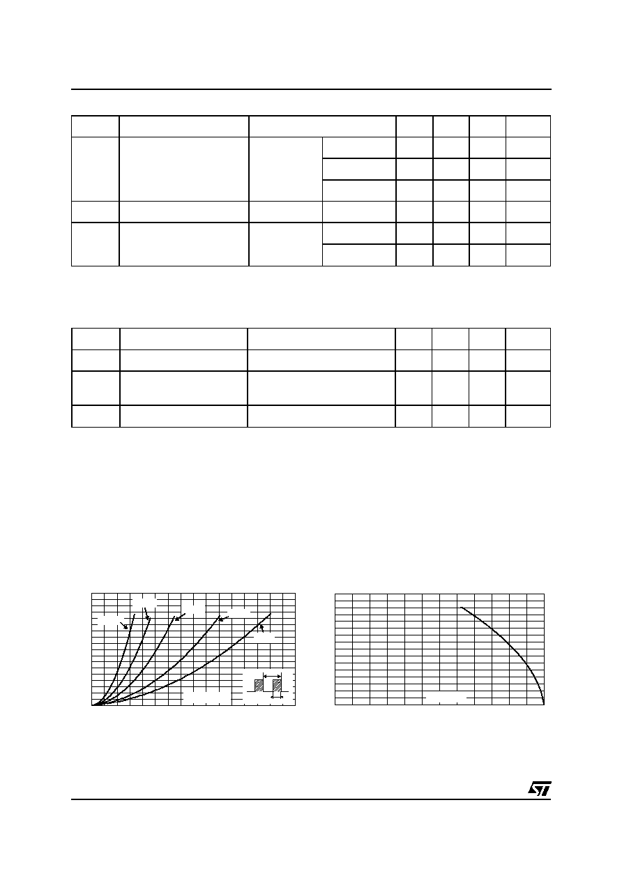
Fig.1 : Average forward power dissipation versus
average forward current.
0
25
50
75
100
125
150
0
10
20
30
40
50
60
70
80
IF(mA)
Tamb(∞C)
Fig.2 : Continuous forward current versus ambient
temperature.
Pulse test:
* tp = 380
µ
s,
< 2%
** tp = 5 ms,
< 2%
BAS70-07
2/4
1E-3
1E-2
1E-1
1E+0
0.00
0.05
0.10
0.15
0.20
0.25
0.30
IM(A)
Ta=50∞C
Ta=25∞C
Ta=100∞C
t(s)
I
M
t
=0.5
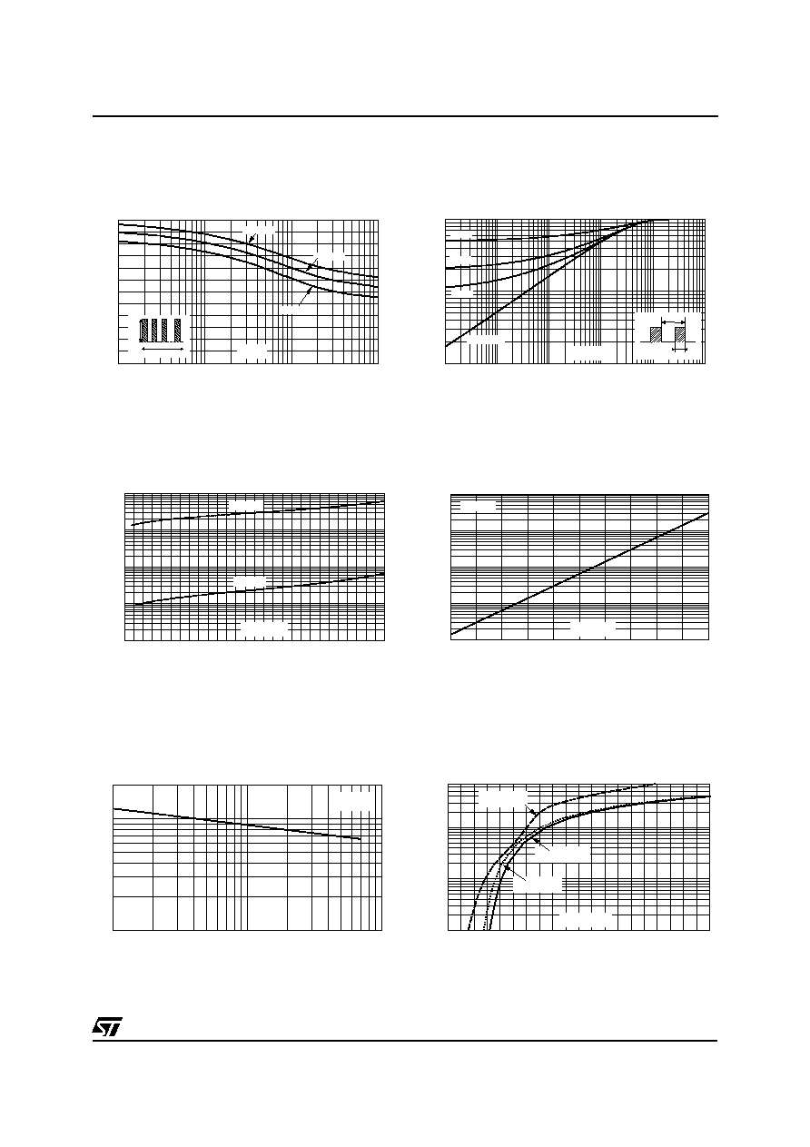
Fig.3 : Non repetitive surge peak forward current
versus overload duration (maximum values).
0
5 10 15 20 25 30 35 40 45 50 55 60 65 70
1E-3
1E-2
1E-1
1E+0
1E+1
IR(µA)
Tj=25∞C
Tj=100∞C
VR(V)
Fig.5 : Reverse leakage current versus reverse
voltage applied (typical values).
1E-3
1E-2
1E-1
1E+0
1E+1
1E+2
0.01
0.10
1.00
Zth(j-a)/Rth(j-a)
tp(s)
T
=tp/T
tp
= 0.1
= 0.2
= 0.5
Single pulse
Fig.4 : Relative variation of thermal impedance
junction to ambient versus pulse duration (alumine
substrate 10mm x 8mm x 0.5mm).
0
25
50
75
100
125
1E-2
1E-1
1E+0
1E+1
1E+2
IR(µA)
VR=70V
Tj(∞C)
Fig.6 : Reverse leakage current versus junction
temperature (typical values).
1
10
100
0.1
1.0
2.0
VR(V)
C(pF)
F=1MHz
Tj=25∞C
Fig.7 : Junction capacitance versus reverse
voltage applied (typical values).
0.0
0.2
0.4
0.6
0.8
1.0
1.2
1.4
1.6
1.8
2.0
1E-4
1E-3
1E-2
7E-2
IFM(A)
Tj=100∞C
Typical values
Tj=25∞C
Maximum values
Tj=25∞C
Typical values
VFM(V)
Fig.8 : Forward voltage drop versus forward
current.
BAS70-07
3/4
Information furnished is believed to be accurate and reliable. However, STMicroelectronics assumes no responsibility for the consequences of
use of such information nor for any infringement of patents or other rights of third parties which may result from its use. No license is granted by
implication or otherwise under any patent or patent rights of STMicroelectronics. Specifications mentioned in this publication are subject to
change without notice. This publication supersedes and replaces all information previously supplied.
STMicroelectronics products are not authorized for use as critical components in life support devices or systems without express written ap-
proval of STMicroelectronics.
The ST logo is a registered trademark of STMicroelectronics
© 1999 STMicroelectronics - Printed in Italy - All rights reserved.
STMicroelectronics GROUP OF COMPANIES
Australia - Brazil - China - Finland - France - Germany - Hong Kong - India - Italy - Japan - Malaysia
Malta - Morocco - Singapore - Spain - Sweden - Switzerland - United Kingdom - U.S.A.
http://www.st.com
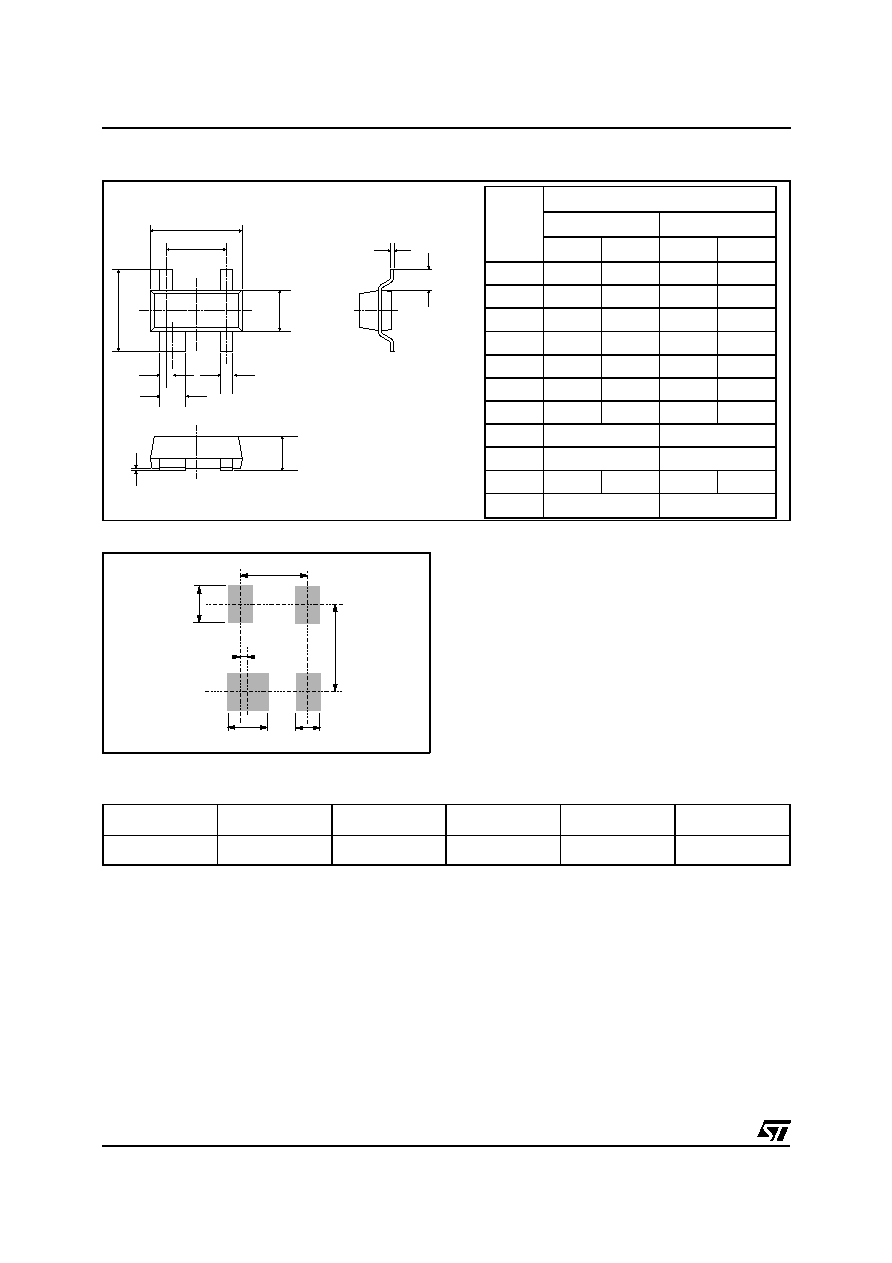
PACKAGE MECHANICAL DATA
SOT-143
A
L
C
D
E
H
e2
b
b1
e1
A1
REF.
DIMENSIONS
Millimeters
Inches
Min.
Max.
Min.
Max.
A
0.8
1.2
0.0314 0.0472
A1
0.01
0.127
0.0004
0.005
b
0.35
0.6
0.014
0.024
b1
0.55
0.95
0.022
0.037
C
0.085
0.2
0.003
0.008
D
2.8
3.04
0.11
0.12
E
1.2
1.4
0.047
0.055
e1
1.90 Typ.
0.075 Typ.
e2
0.2 Typ.
0.008 Typ.
H
2.1
2.64
0.083
0.103
L
0.55 Typ.
0.022 Typ.
FOOTPRINT DIMENSIONS (millimeters)
Type
Marking
Package
Weight
Base qty
Delivery mode
BAS70-07
D99
SOT-143
0.01g.
3000
Tape & reel
MARKING
1.92
0.95
2.25
1.1
0.65
0.2
BAS70-07
4/4