 | –≠–ª–µ–∫—Ç—Ä–æ–Ω–Ω—ã–π –∫–æ–º–ø–æ–Ω–µ–Ω—Ç: BAT54 | –°–∫–∞—á–∞—Ç—å:  PDF PDF  ZIP ZIP |

BAT54, A, C, S
Æ
June 1999 - Ed: 3A
SMALL SIGNAL SCHOTTKY DIODE
VERY SMALL CONDUCTION LOSSES
NEGLIGIBLE SWITCHING LOSSES
LOW FORWARD VOLTAGE DROP
SURFACE MOUNT DEVICE
FEATURES AND BENEFITS
Schottky barrier diodes encapsulated in a SOT-23
small SMD packages.
Double diodes with different pining are available.
DESCRIPTION
SOT-23
K
K
A
A
Nc
Symbol
Parameter
Value
Unit
V
RRM
Repetitive peak reverse voltage
30
V
I
F
Continuous forward current
0.3
A
I
FSM
Surge non repetitive forward current
tp=10ms sinusoidal
1
A
P
tot
Power dissipation (note 1)
T
amb
= 25∞C
250
mW
T
stg
Maximum storage temperature range
- 65 to +150
∞
C
Tj
Maximum operating junction temperature *
150
∞
C
T
L
Maximum temperature for soldering during 10s
260
∞
C
Note 1: for double diodes, Ptot is the total dissipation of both diodes.
ABSOLUTE RATINGS (limiting values)
BAT54
A2
A2
A1
A1
K
K
BAT54C
A2
A2
A1
K2
A1
K2
K1
K1
BAT54S
* :
dPtot
dTj
<
1
Rth
(
j
-
a
)
thermal runaway condition for a diode on its own heatsink
K2
K2
K1
K1
A
A
BAT54A
1/5
Symbol
Parameters
Tests conditions
Min.
Typ.
Max.
Unit
V
F
*
Forward voltage drop
Tj = 25
∞
C
I
F
= 0.1 mA
240
mV
I
F
= 1 mA
320
I
F
= 10 mA
400
I
F
= 30 mA
500
I
F
= 100 mA
900
I
R
**
Reverse leakage current
Tj = 25
∞
C
V
R
= 30 V
1
µ
A
Tj = 100
∞
C
100
Pulse test :
* tp = 380
µ
s,
< 2%
** tp = 5 ms,
< 2%
STATIC ELECTRICAL CHARACTERISTICS (per diode)
Symbol
Parameters
Tests conditions
Min.
Typ.
Max.
Unit
C
Junction
capacitance
Tj = 25
∞
C
V
R
= 1 V
F = 1 MHz
10
pF
t
rr
Reverse recovery
time
I
F
= 10 mA I
R
= 10 mA Tj = 25∞C
I
rr
= 1 mA R
L
= 100
5
ns
DYNAMIC CHARACTERISTICS (Tj = 25 ∞C)
0.00
0.05
0.10
0.15
0.20
0.25
0.30
0.00
0.05
0.10
0.15
0.20
0.25
0.30
0.35
PF(av)(W)
= 0.2
= 0.5
= 1
= 0.05
= 0.1
IF(av) (A)
T
=tp/T
tp
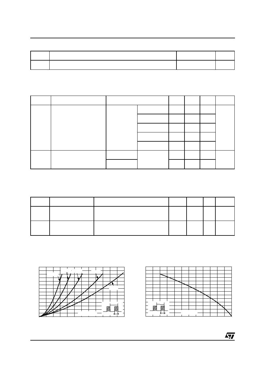
Fig.1 : Average forward power dissipation versus
average forward current.
0
25
50
75
100
125
150
0.00
0.05
0.10
0.15
0.20
0.25
0.30
0.35
IF(av)(A)
T
=tp/T
tp
Tamb(∞C)
Fig.2 : Average forward current versus ambient
temperature (
= 1).
Symbol
Parameter
Value
Unit
R
th (j-a)
Junction to ambient (*)
500
∞
C/W
(*) Mounted on epoxy board with recommended pad layout.
THERMAL RESISTANCE
BAT54, A, C, S
2/5
1E-3
1E-2
1E-1
1E+0
0.0
0.1
0.2
0.3
0.4
0.5
0.6
0.7
0.8
0.9
1.0
IM(A)
Ta=25∞C
Ta=50∞C
Ta=100∞C
I
M
t
=0.5
t(s)
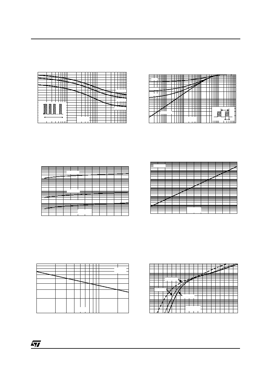
Fig.3 : Non repetitive surge peak forward current
versus overload duration (maximum values).
0
5
10
15
20
25
30
1E-2
1E-1
1E+0
1E+1
1E+2
VR(V)
IR(µA)
Tj=50∞C
Tj=25∞C
Tj=100∞C
Fig.5 : Reverse leakage current versus reverse
voltage applied (typical values).
1E-3
1E-2
1E-1
1E+0
1E+1
1E+2
0.01
0.10
1.00
tp(s)
Zth(j-a)/Rth(j-a)
T
=tp/T
tp
Single pulse
= 0.1
= 0.2
= 0.5
Fig.4 : Relative variation of thermal impedance
junction to ambient versus pulse duration (alumine
substrate 10mm x 8mm x 0.5mm).
0
25
50
75
100
125
150
1E-2
1E-1
1E+0
1E+1
1E+2
1E+3
1E+4
IR(µA)
VR=30V
Tj(∞C)
Fig.6 : Reverse leakage current versus junction
temperature.
1
2
5
10
20
30
1
2
5
10
VR(V)
C(pF)
F=1MHz
Tj=25∞C
Fig.7 : Junction capacitance versus reverse
voltage applied (typical values).
0.0
0.1
0.2
0.3
0.4
0.5
0.6
0.7
0.8
0.9
1.0
1E-4
1E-3
1E-2
1E-1
5E-1
VFM(V)
IFM(A)
Tj=100∞C
Tj=50∞C
Tj=25∞C
Fig.8 : Forward voltage drop versus forward
current (typical values).
BAT54, A, C, S
3/5
PACKAGE MECHANICAL DATA
SOT-23
B
E
S
e
e1
A
D
c
L
H
A1
REF.
DIMENSIONS
Millimeters
Inches
Min.
Max.
Min.
Max.
A
0.89
1.4
0.035
0.055
A1
0
0.1
0
0.004
B
0.3
0.51
0.012
0.02
c
0.085
0.18
0.003
0.007
D
2.75
3.04
0.108
0.12
e
0.85
1.05
0.033
0.041
e1
1.7
2.1
0.067
0.083
E
1.2
1.6
0.047
0.063
H
2.1
2.75
0.083
0.108
L
0.6 typ.
0.024 typ.
S
0.35
0.65
0.014
0.026
Ordering type
Marking
Package
Weight
Base qty
Delivery mode
BAT54FILM
D86
SOT-23
0.01g
3000
Tape & reel
BAT54AFILM
D84
SOT-23
0.01g
3000
Tape & reel
BAT54CFILM
D87
SOT-23
0.01g
3000
Tape & reel
BAT54SFILM
D88
SOT-23
0.01g
3000
Tape & reel
Epoxy meets UL94,V0
BAT54, A, C, S
4/5

Information furnished is believed to be accurate and reliable. However, STMicroelectronics assumes no responsibility for the consequences of
use of such information nor for any infringement of patents or other rights of third parties which may result from its use. No license is granted by
implication or otherwise under any patent or patent rights of STMicroelectronics. Specifications mentioned in this publication are subject to
change without notice. This publication supersedes and replaces all information previously supplied.
STMicroelectronics products are not authorized for use as critical components in life support devices or systems without express written ap-
proval of STMicroelectronics.
The ST logo is a registered trademark of STMicroelectronics
© 1999 STMicroelectronics - Printed in Italy - All rights reserved.
STMicroelectronics GROUP OF COMPANIES
Australia - Brazil - China - Finland - France - Germany - Hong Kong - India - Italy - Japan - Malaysia
Malta - Morocco - Singapore - Spain - Sweden - Switzerland - United Kingdom - U.S.A.
http://www.st.com
0.9
0.035
0.9
0.035
1.9
0.075
mm
inch
2.35
0.92
1.1
0.043
1.1
0.043
1.45
0.037
0.9
0.035
FOOTPRINT DIMENSIONS
COMPATIBLE SOT-23 / SC-59
(in millimeters and inches)
0.9
0.035
0.9
0.035
2
0.079
mm
inch
2.35
0.92
1
0.040
1
0.040
1
0.040
0.9
0.035
OPTIMIZED SOT-23 FOOTPRINT DIMENSIONS
(in millimeters and inches)
BAT54, A, C, S
5/5