BC107
BC108
LOW NOISE GENERAL PURPOSE AUDIO AMPLIFIERS
DESCRIPTION
The BC107 and BC108 are silicon planar
epitaxial NPN transistors in TO-18 metal case.
They are suitable for use in driver stages, low
noise input stages and signal processing circuits
of television reveivers. The PNP complemet for
BC107 is BC177.
INTERNAL SCHEMATIC DIAGRAM
November 1997
ABSOLUTE MAXIMUM RATINGS
Symbol
Parameter
Value
Unit
BC107
BC108
V
CBO
Collect or-Base Voltage (I
E
= 0)
50
30
V
V
CEO
Collect or-Emitt er Voltage (I
B
= 0)
45
20
V
V
EBO
Emitt er-Base Voltage (I
C
= 0)
6
5
V
I
C
Collect or Current
100
mA
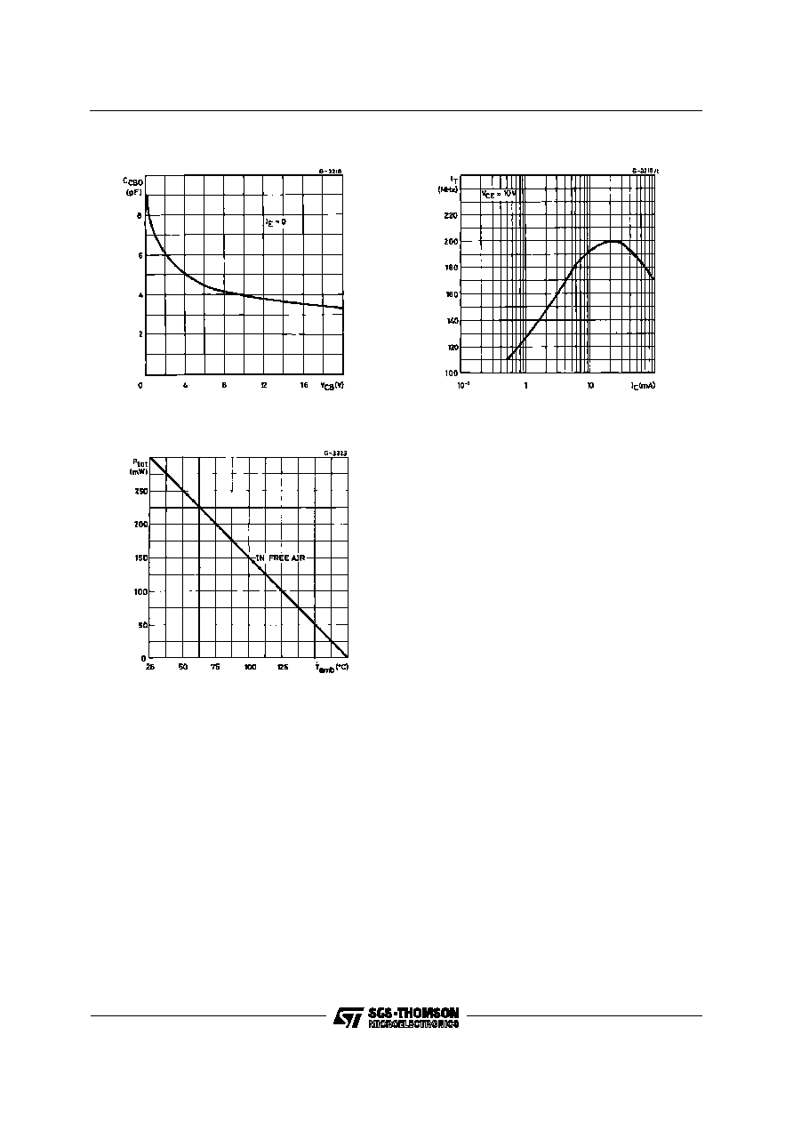
P
t ot
Total Dissipation at T
amb
25
o
C
at T
case
25
o
C
0.3
0.75
W
W
T
stg
St orage Temperature
-55 t o 175
o
C
T
j
Max. Operating Junction Temperature
175
o
C
TO-18
1/6

THERMAL DATA
R
t hj-ca se
R
t hj- amb
Thermal Resistance Junction-Case
Max
Thermal Resistance Junction-Ambient
Max
200
500
o
C/W
o
C/W
ELECTRICAL CHARACTERISTICS (T
case
= 25
o
C unless otherwise specified)
Symb ol
Parameter
Test Cond ition s
Mi n.
Typ .
Max.
Un it
I
CBO
Collect or Cut-off
Current (I
E
= 0)
for BC107
V
CB
= 40 V
V
CB
= 40 V
T
ca s e
= 150
o
C
for BC108
V
CB
= 20 V
V
CB
= 20 V
T
ca s e
= 150
o
C
15
15
15
15
nA
�
A
�
A
�
A
V
(BR)CBO
Collect or-Base
Breakdown Volt age
(I E = 0)
I
C
= 10
�
A
for BC107
for BC108
50
30
V
V
V
( BR)CEO
Collect or-Emitter
Breakdown Volt age
(I
B
= 0)
I
C
= 10 mA
for BC107
for BC108
45
20
V
V
V
(BR)EBO
Emitt er-Base
Breakdown Volt age
(I
C
= 0)
I
E
= 10
�
A
for BC107
for BC108
6
5
V
V
V
CE(sat )
Collect or-Emitter
Saturat ion Voltage
I
C
= 10 mA
I
B
= 0.5 mA
I
C
= 100 mA
I
B
= 5 mA
70
200
250
600
mV
mV
V
BE(s at)
Base-Emitt er
Saturat ion Voltage
I
C
= 10 mA
I
B
= 0.5 mA
I
C
= 100 mA
I
B
= 5 mA
750
950
mV
mV
V
BE(on)
Base-Emitt er O n
Voltage
I
C
= 2 mA
V
CE
= 5 V
I
C
= 10 mA
V
CE
= 5 V
550
650
700
700
770
mV
mV
h
FE
DC Current G ain
I
C
= 2 mA
V
CE
= 5 V
for BC107
for BC107 Gr. A
for BC107 Gr. B
for BC108
for BC108 Gr. A
for BC108 Gr. B
for BC108 Gr. C
I
C
= 10
�
A
V
CE
= 5 V
for BC107
for BC107 Gr. A
for BC107 Gr. B
for BC108
for BC108 Gr. A
for BC108 Gr. B
for BC108 Gr. C
110
110
200
110
110
200
420
40
40
100
120
90
150
120
90
150
270
450
220
450
800
220
450
800
h
fe
Small Signal Current
Gain
I
C
= 2 mA
V
CE
= 5 V
f = 1KHz
for BC107
for BC107 Gr. A
for BC107 Gr. B
for BC108
for BC108 Gr. A
for BC108 Gr. B
for BC108 Gr. C
I
C
= 10 mA V
CE
= 10 V f = 100 MHz
250
190
300
370
190
300
500
2
Pulsed: Pulse duration = 300
�
s, duty cycle
1 %
BC107/BC108
2/6
ELECTRICAL CHARACTERISTICS (continued)
Symb ol
Parameter
Test Cond ition s
Mi n.
Typ .
Max.
Un it
C
CBO
Collect or Base
Capacitance
I
E
= 0
V
CB
= 10 V
f = 1MHz
4
6
pF
C
EBO
Emitt er Base
Capacitance
I
C
= 0
V
EB
= 0.5 V
f = 1MHz
12
pF
NF
Noise Figure
I
C
= 0. 2 mA
V
CE
= 5 V
f = 1KHz
R
g
= 2K
B = 200Hz
2
10
dB
h
ie
Input Impedance
I
C
= 2 mA
V
CE
= 5 V
f = 1KHz
for BC107
for BC107 Gr. A
for BC107 Gr. B
for BC108
for BC108 Gr. A
for BC108 Gr. B
for BC108 Gr. C
4
3
4.8
5.5
3
4.8
7
K
K
K
K
K
K
K
h
re
Reverse Voltage Ratio
I
C
= 2 mA
V
CE
= 5 V
f = 1KHz
for BC107
for BC107 Gr. A
for BC107 Gr. B
for BC108
for BC108 Gr. A
for BC108 Gr. B
for BC108 Gr. C
2.2
1.7
2.7
3.1
1.7
2.7
3.8
10
-4
10
-4
10
-4
10
-4
10
-4
10
-4
10
-4
h
oe
Output Admittance
I
C
= 2 mA
V
CE
= 5 V
f = 1KHz
for BC107
for BC107 Gr. A
for BC107 Gr. B
for BC108
for BC108 Gr. A
for BC108 Gr. B
for BC108 Gr. C
30
13
26
30
13
26
34
�
S
�
S
�
S
�
S
�
S
�
S
�
S
Pulsed: Pulse duration = 300
�
s, duty cycle
1 %
DC Normalized Current Gain.
Collector--emitter Saturation Voltage.
BC107/BC108
3/6