 | –≠–ª–µ–∫—Ç—Ä–æ–Ω–Ω—ã–π –∫–æ–º–ø–æ–Ω–µ–Ω—Ç: BDW94C | –°–∫–∞—á–∞—Ç—å:  PDF PDF  ZIP ZIP |
BDW93C
BDW94B/BDW94C
COMPLEMENTARY SILICON POWER
DARLINGTON TRANSISTORS
s
STMicroelectronics PREFERRED
SALESTYPES
s
COMPLEMENTARY PNP - NPN DEVICES
s
INTEGRATED ANTIPARALLEL
COLLECTOR-EMITTER DIODE
APPLICATIONS
s
LINEAR AND SWITCHING INDUSTRIAL
EQUIPMENT
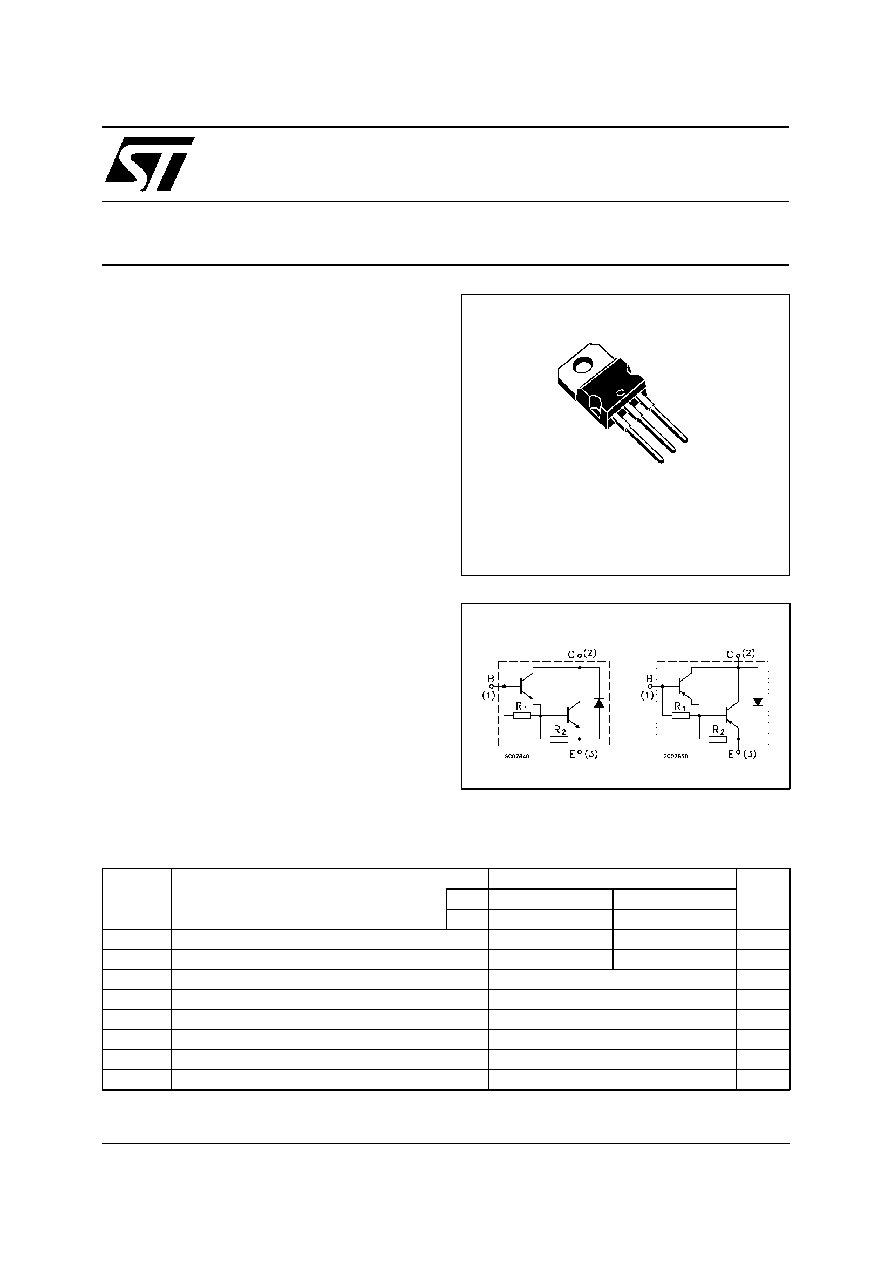
DESCRIPTION
The BDW93C is a silicon Epitaxial-Base NPN
power
transistor
in
monolithic
Darlington
configuration mounted in Jedec TO-220 plastic
package. It is intented for use in power linear and
switching applications.
The complementary PNP type is BDW94C.
Also BDW94B is a PNP type.
Æ
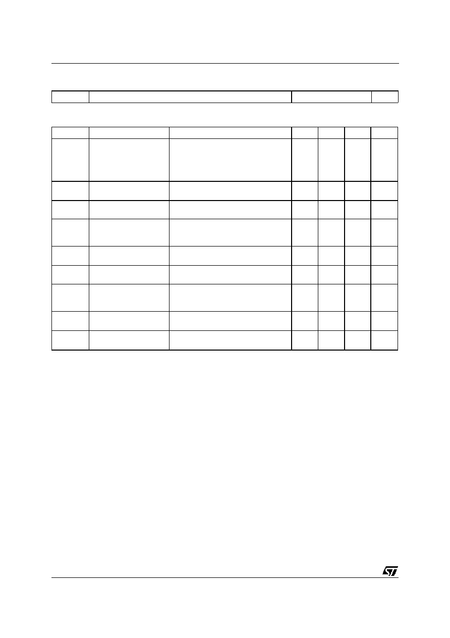
INTERNAL SCHEMATIC DIAGRAM
October 1999
ABSOLUTE MAXIMUM RATINGS
Symbol
Parameter
Val ue
Un it
NPN
BDW93C
PNP
BDW94B
BDW94C
V
CBO
Collector-Base Voltage (I
E
= 0)
80
100
V
V
CEO
Collector-Emitter Voltage (I
B
= 0)
80
100
V
I
C
Collector Current
12
A
I
CM
Collector Peak Current
15
A
I
B
Base Current
0.2
A
P
tot
T otal Dissipat ion at T
c
25
o
C
80
W
T
s tg
Storage Temperature
-65 t o 150
o
C
T
j
Max. Operating Junction Temperature
150
o
C
For PNP types voltage and current values are negative.
1
2
3
TO-220
R
1
Typ. = 10 K
R
2
Typ. = 150
1/6
THERMAL DATA
R
thj -case
Thermal Resistance Junction-case
1.56
o
C/W
ELECTRICAL CHARACTERISTICS (T
case
= 25
o
C unless otherwise specified)
Symbo l
Parameter
Test Con ditions
Min.
Typ.
Max.
Unit
I
CBO
Collector Cut-of f
Current (I
E
= 0)
for BDW94B
V
CB
= 80 V
for BDW93C/94C
V
CB
= 100 V
T
case
= 150
o
C
for BDW94B
V
CB
= 80 V
for BDW93C/94C
V
CB
= 100 V
100
100
5
5
µ
A
µ
A
mA
mA
I
CEO
Collector Cut-of f
Current (I
B
= 0)
for BDW94B
V
CE
= 80 V
for BDW93C/94C
V
CE
= 100 V
1
1
mA
mA
I
EBO
Emitter Cut-of f Current
(I
C
= 0)
V
EB
= 5 V
2
mA
V
CEO (s us)
Collector-Emitt er
Sustaining Volt age
(I
B
= 0)
I
C
= 100 mA
for BDW94B
for BDW 93C/94C
80
100
V
V
V
CE(sat)
Collector-Emitt er
Sat uration Voltage
I
C
= 5 A
I
B
= 20 mA
I
C
= 10 A
I
B
= 100 mA
2
3
V
V
V
BE(sat)
Base-Emitter
Sat uration Voltage
I
C
= 5 A
I
B
= 20 mA
I
C
= 10 A
I
B
= 100 mA
2. 5
4
V
V
h
FE
DC Current G ain
I
C
= 3 A
V
CE
= 3 V
I
C
= 5 A
V
CE
= 3 V
I
C
= 10 A
V
CE
= 3 V
1000
750
100
20K
V
F
*
Parallel-diode Forward
Voltage
I
F
= 5 A
I
F
= 10 A
1.3
1.8
2
4
V
V
h
fe
Small Signal Current
Gain
I
C
= 1 A
V
CE
= 10 V
f = 1 MHz
20
Pulsed: Pulse duration = 300
µ
s, duty cycle 1.5 %
For PNP types voltage and current values are negative.
BDW93C/BDW94B/BDW94C
2/6
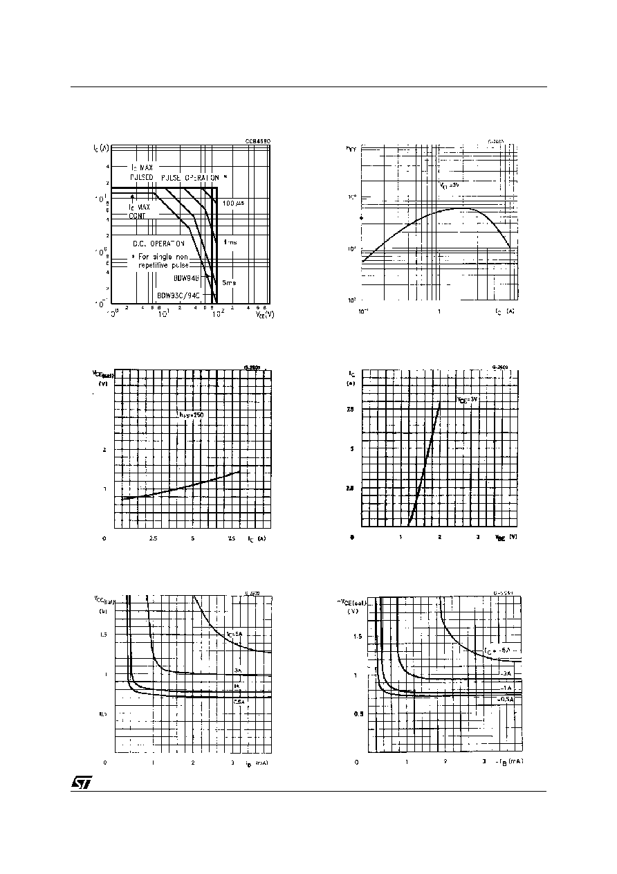
Safe Operating Area
Collector Emitter Saturation Voltage (NPN types)
Collector Emitter Saturation Voltage (NPN types)
DC Current Gain (NPN types)
DC Transconductance(NPN types)
Collector Emitter Saturation Voltage (PNP types)
BDW93C/BDW94B/BDW94C
3/6
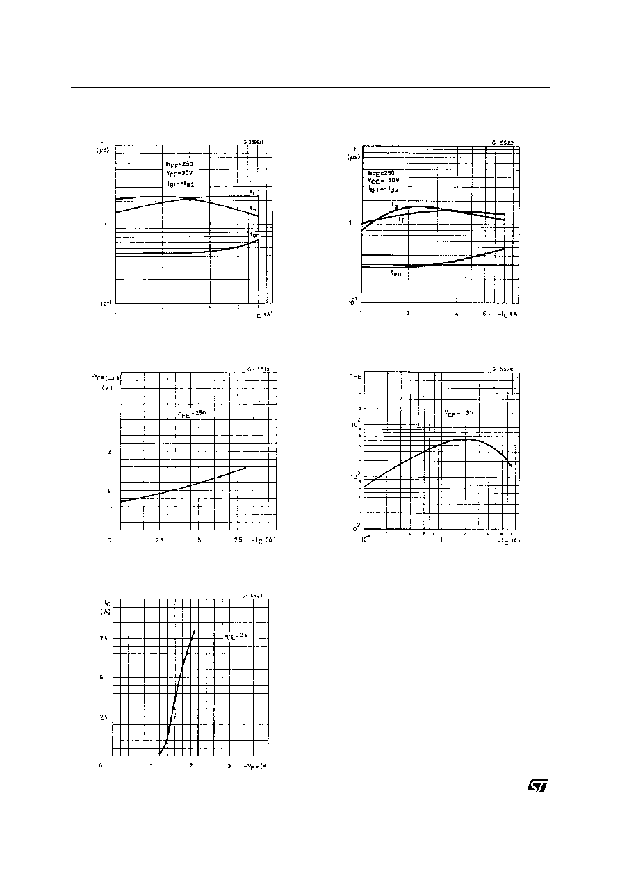
Saturated Switching Characteristics (NPN types)
Collector Emitter Saturation Voltage (PNP types)
Saturated Switching Characteristics (PNP types)
DC Current Gain (PNP types)
DC Transconductance(PNP types)
BDW93C/BDW94B/BDW94C
4/6
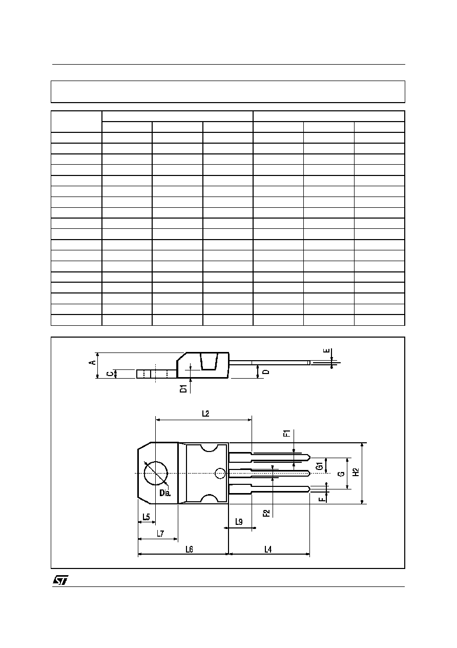
DIM.
mm
inch
MIN.
TYP.
MAX.
MIN.
TYP.
MAX.
A
4.40
4.60
0.173
0.181
C
1.23
1.32
0.048
0.051
D
2.40
2.72
0.094
0.107
D1
1.27
0.050
E
0.49
0.70
0.019
0.027
F
0.61
0.88
0.024
0.034
F1
1.14
1.70
0.044
0.067
F2
1.14
1.70
0.044
0.067
G
4.95
5.15
0.194
0.203
G1
2.4
2.7
0.094
0.106
H2
10.0
10.40
0.393
0.409
L2
16.4
0.645
L4
13.0
14.0
0.511
0.551
L5
2.65
2.95
0.104
0.116
L6
15.25
15.75
0.600
0.620
L7
6.2
6.6
0.244
0.260
L9
3.5
3.93
0.137
0.154
DIA.
3.75
3.85
0.147
0.151
P011C
TO-220 MECHANICAL DATA
BDW93C/BDW94B/BDW94C
5/6