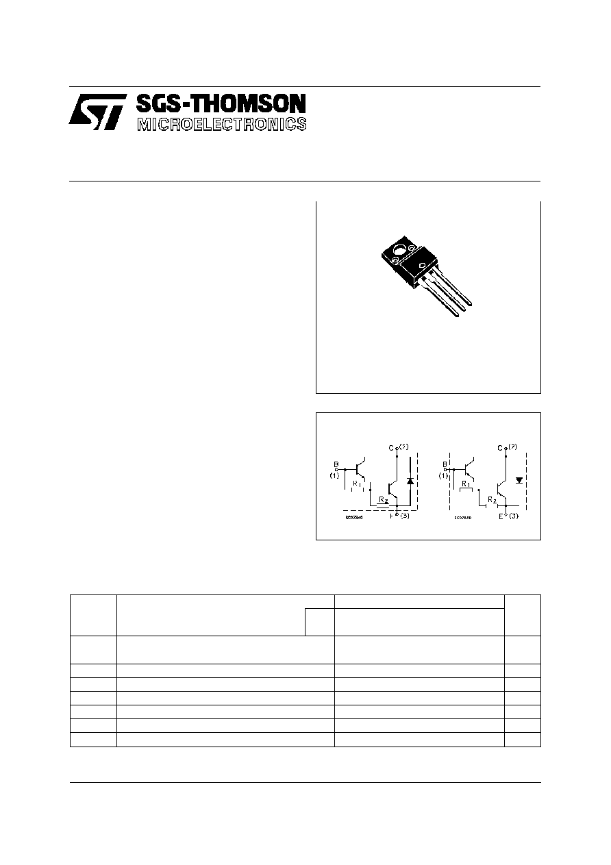
BDW93CFP
BDW94CFP
COMPLEMENTARY SILICON POWER
DARLINGTON TRANSISTORS
s
SGS-THOMSON PREFERRED SALESTYPES
s
MONOLITHIC DARLINGTON
CONFIGURATION
s
COMPLEMENTARY PNP - NPN DEVICES
s
INTEGRATED ANTIPARALLEL
COLLECTOR-EMITTER DIODE
s
FULLY MOLDED ISOLATED PACKAGE
s
2000 V DC ISOLATION (U.L. COMPLIANT)
APPLICATIONS
s
LINEAR AND SWITCHING INDUSTRIAL
EQUIPMENT
DESCRIPTION
The BDW93CFP, is a silicon epitaxial-base NPN
transistor in monolithic Darlington configuration
and is mounted in TO-220FP fully molded
isolated package. It is intented for use in power
linear and switching applications.
The complementary PNP type is the BDW94CFP.
INTERNAL SCHEMATIC DIAGRAM
April 1998
ABSOLUTE MAXIMUM RATINGS
Symbol
Parameter
Val ue
Uni t
NPN
BDW 93CFP
PNP
BDW 94CFP
V
CBO
Collector-Base Voltage (I
E
= 0)
100
V
V
CEO
Collector-Emit ter Voltage (I
B
= 0)
100
V
I
C
Collector Current
12
A
I
CM
Collector Peak Current
15
A
I
B
Base Current
0.2
A
P
t ot
Tot al Dissipation at T
c
25
o
C
33
W
T
stg
Storage Temperature
-65 to 150
o
C
T
j
Max. O perat ing Junction Temperature
150
o
C
For PNP types voltage and current values are negative.
R
1
Typ. = 10 K
R
2
Typ. = 150
1
2
3
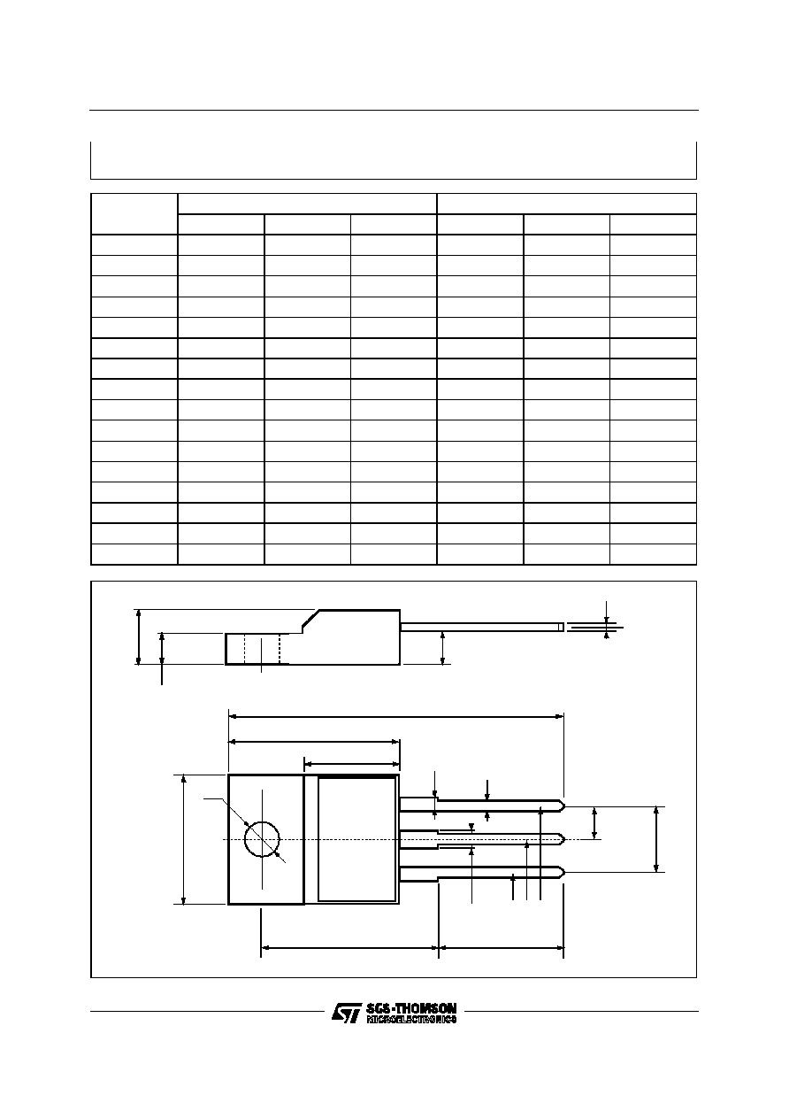
T0-220FP
1/4
THERMAL DATA
R
t hj-ca se
Thermal Resistance Junction-case
3.8
o
C/W
ELECTRICAL CHARACTERISTICS (T
case
= 25
o
C unless otherwise specified)
Symb ol
Parameter
Test Cond ition s
Mi n.
Typ .
Max.
Un it
I
CBO
Collect or Cut-off
Current (I
E
= 0)
V
CB
= 100 V
V
CB
= 100 V
T
case
= 150
o
C
100
5
µ
A
mA
I
CEO
Collect or Cut-off
Current (I
B
= 0)
V
CE
= 80 V
1
mA
I
EBO
Emitt er Cut-off Current
(I
C
= 0)
V
EB
= 5 V
2
mA
V
CEO(sus )
Collect or-Emitter
Sustaining Voltage
(I
B
= 0)
I
C
= 100 mA
100
V
V
CE(sat )
Collect or-Emitter
Saturat ion Voltage
I
C
= 5 A
I
B
= 20 mA
I
C
= 10 A
I
B
= 100 mA
2
3
V
V
V
BE(s at)
Base-Emitt er
Saturat ion Voltage
I
C
= 5 A
I
B
= 20 mA
I
C
= 10 A
I
B
= 100 mA
2.5
4
V
V
h
FE
DC Current G ain
I
C
= 3 A
V
CE
= 3 V
I
C
= 5 A
V
CE
= 3 V
I
C
= 10 A
V
CE
= 3 V
1000
750
100
20000
V
F
*
Parallel-diode Forward
Voltage
I
F
= 5 A
I
F
= 10 A
1.3
1.8
2
4
V
V
h
f e
Small Signal Current
Gain
IC = 1 A
V
CE
= 10 V
f = 1 MHz
20
Pulsed: Pulse duration = 300
µ
s, duty cycle 1.5 %
For PNP types voltage and current values are negative.
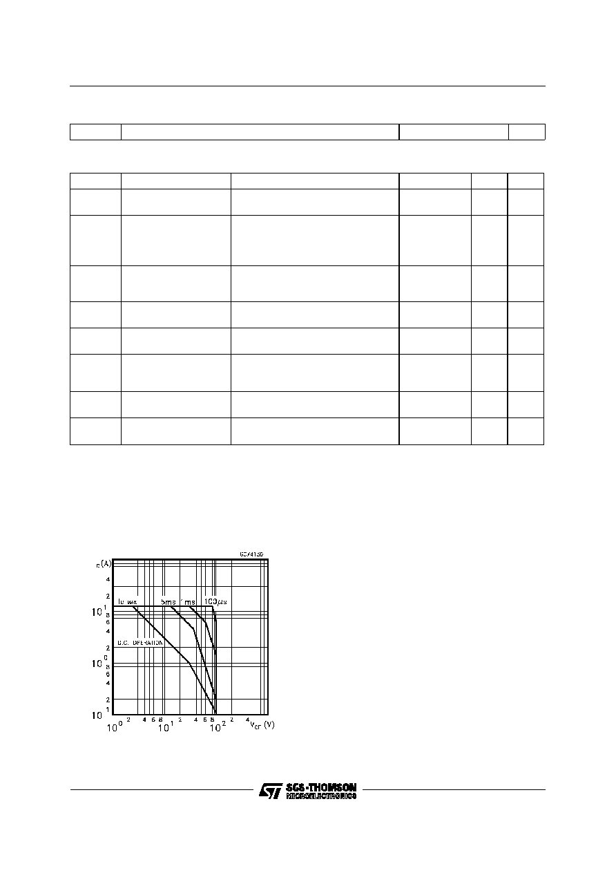
Safe Operating Area
BDW93CFP / BDW94CFP
2/4

Information furnished is believed to be accurate and reliable. However, SGS-THOMSON Microelectronics assumes no responsability for the
consequences of use of such information nor for any infringement of patents or other rights of third parties which may results from its use. No
license is granted by implication or otherwise under any patent or patent rights of SGS-THOMSON Microelectronics. Specifications mentioned
in this publication are subject to change without notice. This publication supersedes and replaces all information previously supplied.
SGS-THOMSON Microelectronics products are not authorized for use as critical components in life support devices or systems without express
written approval of SGS-THOMSON Microelectonics.
©
1998 SGS-THOMSON Microelectronics - Printed in Italy - All Rights Reserved
SGS-THOMSON Microelectronics GROUP OF COMPANIES
Australia - Brazil - Canada - China - France - Germany - Italy - Japan - Korea - Malaysia - Malta - Morocco - The Netherlands -
Singapore - Spain - Sweden - Switzerland - Taiwan - Thailand - United Kingdom - U.S.A
. . .
BDW93CFP / BDW94CFP
4/4