BDX53B / BDX53C
BDX54B / BDX54C
COMPLEMENTARY SILICON POWER
DARLINGTON TRANSISTORS
s
STMicroelectronics PREFERRED
SALESTYPES
APPLICATIONS
s
AUDIO AMPLIFIERS
s
LINEAR AND SWITCHING INDUSTRIAL
EQUIPMENT
DESCRIPTION
The
BDX53B
and
BDX53C
are
silicon
Epitaxial-Base
NPN
power
transistors
in
monolithic Darlington configuration mounted in
Jedec TO-220 plastic package. They are intented
for use in hammer drivers, audio amplifiers and
other
medium
power
linear
and
switching
applications.
The complementary PNP types are BDX54B and
BDX54C respectively.
�
INTERNAL SCHEMATIC DIAGRAM
September 1999
ABSOLUTE MAXIMUM RATINGS
Symbol
Parameter
Val ue
Un it
NPN
BDX53B
BDX53C
PNP
BDX54B
BDX54C
V
CBO
Collector-Base Voltage (I
E
= 0)
80
100
V
V
CEO
Collector-Emitter Voltage (I
B
= 0)
80
100
V
V
EBO
Emitter-base Voltage (I
C
= 0)
5
V
I
C
Collector Current
8
A
I
CM
Collector Peak Current (repetitive)
12
A
I
B
Base Current
0.2
A
P
tot
T otal Dissipation at T
c
25
o
C
60
W
T
s tg
Storage Temperat ure
-65 t o 150
o
C
T
j
Max. Operating Junction Temperature
150
o
C
For PNP types voltage and current values are negative.
1
2
3
TO-220
R
1
Typ. = 10 K
R
2
Typ. = 150
1/6

THERMAL DATA
R
thj -case
R
thj -amb
Thermal Resistance Junction-case
Max
Thermal Resistance Junction-ambient
Max
2.08
70
o
C/W
o
C/W
ELECTRICAL CHARACTERISTICS (T
case
= 25
o
C unless otherwise specified)
Symbo l
Parameter
Test Con ditions
Min.
T yp.
Max.
Unit
I
CBO
Collector Cut -of f
Current (I
E
= 0)
for BDX53B/54B
V
CB
= 80 V
for BDX53C/54C
V
CB
= 100V
0. 2
0. 2
mA
mA
I
CEO
Collector Cut -of f
Current (I
B
= 0)
for BDX53B/54B
V
CE
= 40 V
for BDX53C/54C
V
CE
= 50V
0. 5
0. 5
mA
mA
I
EBO
Emitter Cut-off Current
(I
C
= 0)
V
EB
= 5 V
2
mA
V
CEO (s us)
Collector-Emitter
Sustaining Voltage
(I
B
= 0)
I
C
= 100 mA
for BDX53B/ 54B
f or BDX53C/54C
80
100
V
V
V
CE(sat)
Collector-emit ter
Sat uration Volt age
I
C
= 3 A
I
B
=12 mA
2
V
V
BE(sat)
Base-emitter
Sat uration Volt age
I
C
= 3 A
I
B
=12 mA
2. 5
V
h
F E
DC Current Gain
I
C
= 3 A
V
CE
= 3 V
750
V
F
Parallel-diode Forward
Voltage
I
F
= 3 A
I
F
= 8 A
1.8
2.5
2. 5
V
V
Pulsed: Pulse duration = 300
�
s, duty cycle 1.5 %
For PNP types voltage and current values are negative.
Safe Operating Area
Derating Curve
BDX53B - BDX53C - BDX54B - BDX54C
2/6

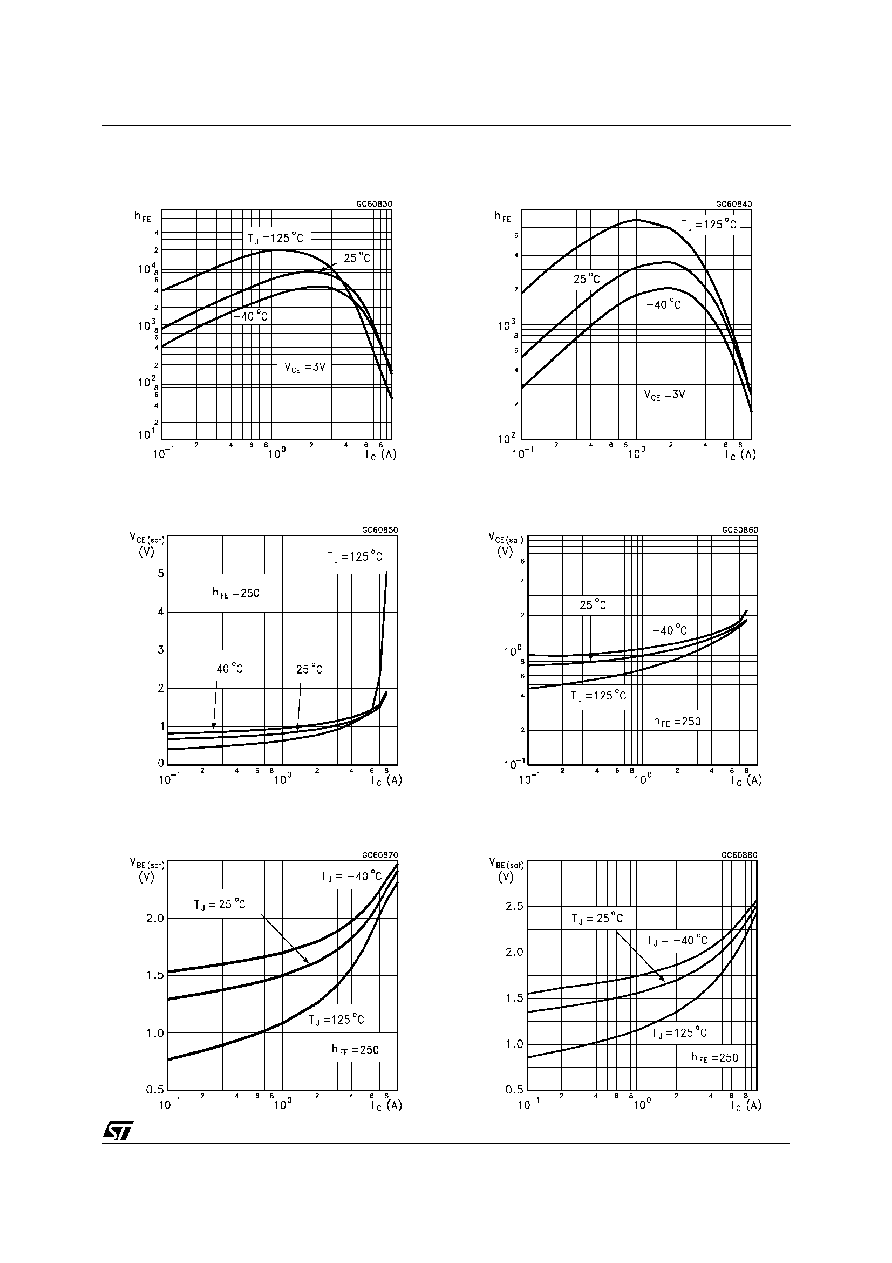
DC Current Gain (NPN type)
Collector Emitter Saturation Voltage (NPN type)
Base Emitter Saturation Voltage (NPN type)
DC Current Gain (PNP type)
Collector Emitter Saturation Voltage (PNP type)
Base Emitter Saturation Voltage (PNP type)
BDX53B - BDX53C - BDX54B - BDX54C
3/6

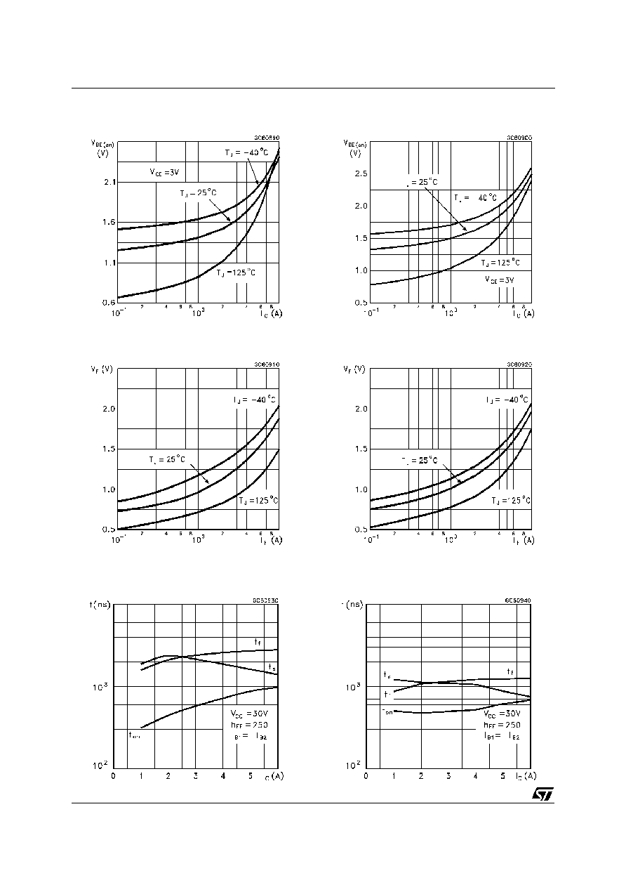
Base Emitter On Voltage (NPN type)
Freewheel Diode Forward Voltage (NPN type)
Base Emitter On Voltage (PNP type)
Freewheel Diode Forward Voltage (PNP type)
Switching Time Resistive Load (NPN type)
Switching Time resistive Load (PNP type)
BDX53B - BDX53C - BDX54B - BDX54C
4/6

DIM.
mm
inch
MIN.
TYP.
MAX.
MIN.
TYP.
MAX.
A
4.40
4.60
0.173
0.181
C
1.23
1.32
0.048
0.051
D
2.40
2.72
0.094
0.107
D1
1.27
0.050
E
0.49
0.70
0.019
0.027
F
0.61
0.88
0.024
0.034
F1
1.14
1.70
0.044
0.067
F2
1.14
1.70
0.044
0.067
G
4.95
5.15
0.194
0.203
G1
2.4
2.7
0.094
0.106
H2
10.0
10.40
0.393
0.409
L2
16.4
0.645
L4
13.0
14.0
0.511
0.551
L5
2.65
2.95
0.104
0.116
L6
15.25
15.75
0.600
0.620
L7
6.2
6.6
0.244
0.260
L9
3.5
3.93
0.137
0.154
DIA.
3.75
3.85
0.147
0.151
P011C
TO-220 MECHANICAL DATA
BDX53B - BDX53C - BDX54B - BDX54C
5/6


