 | –≠–ª–µ–∫—Ç—Ä–æ–Ω–Ω—ã–π –∫–æ–º–ø–æ–Ω–µ–Ω—Ç: BTA12 | –°–∫–∞—á–∞—Ç—å:  PDF PDF  ZIP ZIP |
1/7
Æ
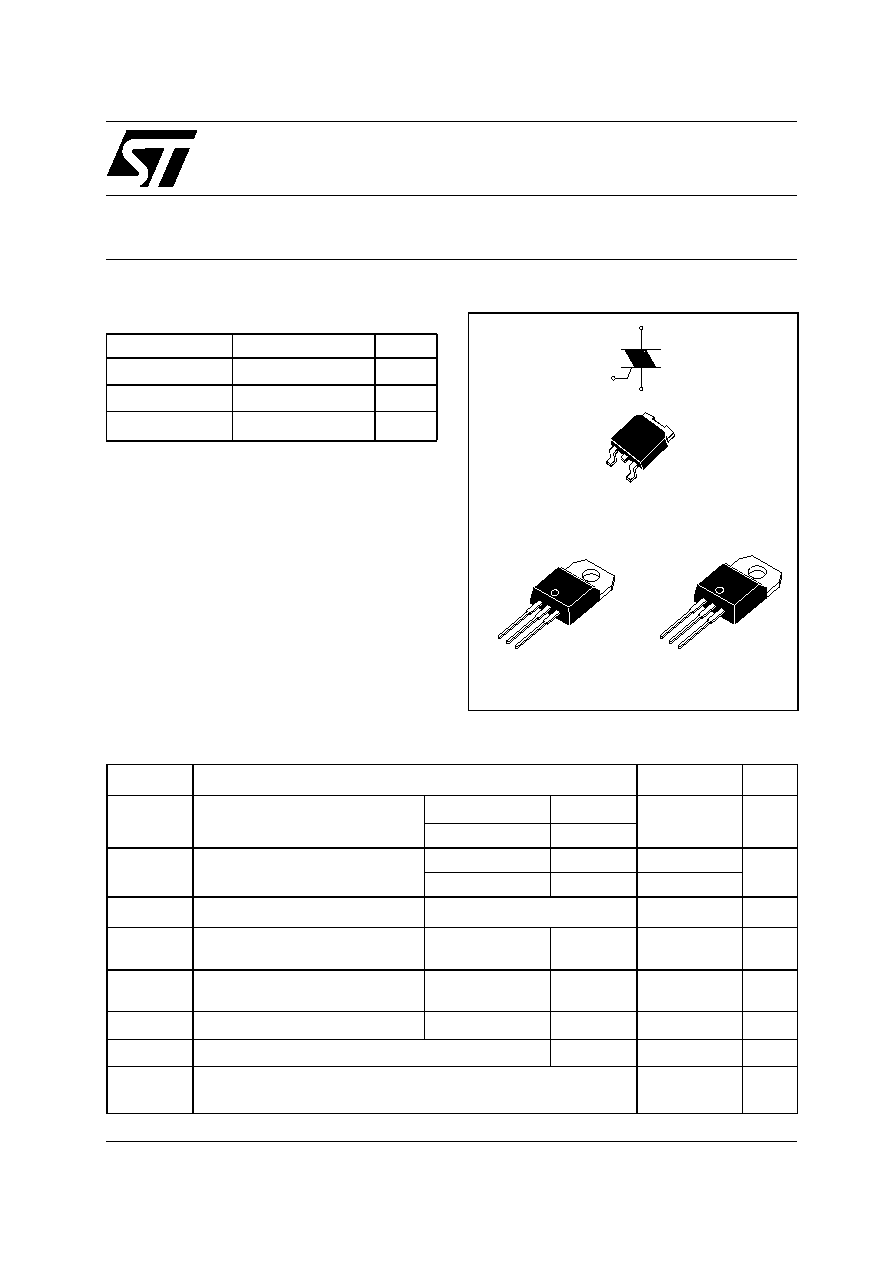
BTA/BTB12 and T12 Series
SNUBBERLESSTM, LOGIC LEVEL & STANDARD
12A TRIAC
S
September 2002 - Ed: 6A
MAIN FEATURES:
DESCRIPTION
Available either in through-hole or surface-mount
packages, the BTA/BTB12 and T12 triac series is
suitable for general purpose AC switching. They
can be used as an ON/OFF function in
applications such as static relays, heating
regulation, induction motor starting circuits... or for
phase control operation in light dimmers, motor
speed controllers,...
The snubberless versions (BTA/BTB...W and T12
series) are specially recommended for use on
inductive loads, thanks to their high commutation
performances. Logic level versions are designed
to interface directly with low power drivers such as
microcontrollers. By using an internal ceramic
pad, the BTA series provides voltage insulated tab
(rated at 2500V RMS) complying with UL
standards (File ref.: E81734)
Symbol
Value
Unit
I
T(RMS)
12
A
V
DRM
/V
RRM
600 and 800
V
I
GT (Q
1
)
5 to 50
mA
ABSOLUTE MAXIMUM RATINGS
Symbol
Parameter
Value
Unit
I
T(RMS)
RMS on-state current (full sine wave)
D
≤
PAK/TO-220AB
Tc = 105∞C
12
A
TO-220AB Ins.
Tc = 90∞C
I
TSM
Non repetitive surge peak on-state
current (full cycle, Tj initial = 25∞C)
F = 50 Hz
t = 20 ms
120
A
F = 60 Hz
t = 16.7 ms
126
I
≤
t
I
≤
t Value for fusing
tp = 10 ms
78
A
≤
s
dI/dt
Critical rate of rise of on-state current
I
G
= 2 x I
GT
, tr
100 ns
F = 120 Hz
Tj = 125∞C
50
A/µs
V
DSM
/V
RSM
Non repetitive surge peak off-state
voltage
tp = 10 ms
Tj = 25∞C
V
DRM
/V
RRM
+ 100
V
I
GM
Peak gate current
tp = 20 µs
Tj = 125∞C
4
A
P
G(AV)
Average gate power dissipation
Tj = 125∞C
1
W
T
stg
T
j
Storage junction temperature range
Operating junction temperature range
- 40 to + 150
- 40 to + 125
∞C
G
A2
A1
G
A2
A2
A1
A2
A2
A1
G
D
2
PAK
(T12-G)
G
A2
A1
TO-220AB Insulated
(BTA12)
TO-220AB
(BTB12)
BTA/BTB12 and T12 Series
2/7
ELECTRICAL CHARACTERISTICS (Tj = 25∞C, unless otherwise specified)
s
SNUBBERLESSTM and LOGIC LEVEL (3 Quadrants)
s
STANDARD (4 Quadrants)
STATIC CHARACTERISTICS
Note 1: minimum IGT is guaranted at 5% of IGT max.
Note 2: for both polarities of A2 referenced to A1
Symbol
Test Conditions
Quadrant
T12
BTA/BTB12
Unit
T1235
TW
SW
CW
BW
I
GT
(1)
V
D
= 12 V R
L
= 30
I - II - III
MAX.
35
5
10
35
50
mA
V
GT
I - II - III
MAX.
1.3
V
V
GD
V
D
= V
DRM
R
L
= 3.3 k
Tj = 125∞C
I - II - III
MIN.
0.2
V
I
H
(2)
I
T
= 100 mA
MAX.
35
10
15
35
50
mA
I
L
I
G
= 1.2 I
GT
I - III
MAX.
50
10
25
50
70
mA
II
60
15
30
60
80
dV/dt (2)
V
D
= 67 %V
DRM
gate open
Tj = 125∞C
MIN.
500
20
40
500
1000
V/µs
(dI/dt)c (2) (dV/dt)c = 0.1 V/µs Tj = 125∞C
MIN.
-
3.5
6.5
-
-
A/ms
(dV/dt)c = 10 V/µs Tj = 125∞C
-
1
2.9
-
-
Without snubber Tj = 125∞C
6.5
-
-
6.5
12
Symbol
Test Conditions
Quadrant
BTA/BTB12
Unit
C
B
I
GT
(1)
V
D
= 12 V R
L
= 30
I - II - III
IV
MAX.
25
50
50
100
mA
V
GT
ALL
MAX.
1.3
V
V
GD
V
D
= V
DRM
R
L
= 3.3 k
Tj = 125∞C
ALL
MIN.
0.2
V
I
H
(2)
I
T
= 500 mA
MAX.
25
50
mA
I
L
I
G
= 1.2 I
GT
I - III - IV
MAX.
40
50
mA
II
80
100
dV/dt (2)
V
D
= 67 %V
DRM
gate open Tj = 125∞C
MIN.
200
400
V/µs
(dV/dt)c (2) (dI/dt)c = 5.3 A/ms Tj = 125∞C
MIN.
5
10
V/µs
Symbol
Test Conditions
Value
Unit
V
T
(2)
I
TM
= 17 A tp = 380 µs
Tj = 25∞C
MAX.
1.55
V
V
to
(2)
Threshold voltage
Tj = 125∞C
MAX.
0.85
V
R
d
(2)
Dynamic resistance
Tj = 125∞C
MAX.
35
m
I
DRM
I
RRM
V
DRM
= V
RRM
Tj = 25∞C
MAX.
5
µA
Tj = 125∞C
1
mA

BTA/BTB12 and T12 Series
3/7
THERMAL RESISTANCES
S = Copper surface under tab
PRODUCT SELECTOR
BTB: non insulated TO-220AB package
ORDERING INFORMATION
Symbol
Parameter
Value
Unit
R
th(j-c)
Junction to case (AC)
D
≤
PAK/TO-220AB
1.4
∞C/W
TO-220AB Insulated
2.3
R
th(j-a)
Junction to ambient
S = 1 cm
≤
D
≤
PAK
45
∞C/W
TO-220AB
TO-220AB Insulated
60
Part Number
Voltage (xxx)
Sensitivity
Type
Package
600 V
800 V
BTA/BTB12-xxxB
X
X
50 mA
Standard
TO-220AB
BTA/BTB12-xxxBW
X
X
50 mA
Snubberless
TO-220AB
BTA/BTB12-xxxC
X
X
25 mA
Standard
TO-220AB
BTA/BTB12-xxxCW
X
X
35 mA
Snubberless
TO-220AB
BTA/BTB12-xxxSW
X
X
10 mA
Logic level
TO-220AB
BTA/BTB12-xxxTW
X
X
5 mA
Logic Level
TO-220AB
T1235-xxxG
X
X
35 mA
Snubberless
D
≤
PAK
BT A 12 - 600 BW (RG)
TRIAC
SERIES
INSULATION:
A: insulated
B: non insulated
CURRENT: 12A
SENSITIVITY & TYPE
B: 50mA STANDARD
BW: 50mA SNUBBERLESS
C: 25mA STANDARD
CW: 35mA SNUBBERLESS
SW: 10mA LOGIC LEVEL
TW: 5mA LOGIC LEVEL
VOLTAGE:
600: 600V
800: 800V
PACKING MODE
Blank: Bulk
RG: Tube
T 12 35 - 600 G (-TR)
TRIAC
SERIES
SENSITIVITY:
35: 35mA
VOLTAGE:
600: 600V
800: 800V
CURRENT: 12A
PACKAGE:
G: D PAK
2
PACKING MODE:
Blank: Tube
-TR: Tape & Reel
BTA/BTB12 and T12 Series
4/7
OTHER INFORMATION
Note: xxx = voltage, yy = sensitivity, z = type
Part Number
Marking
Weight
Base
quantity
Packing
mode
BTA/BTB12-xxxyz
BTA/BTB12-xxxyz
2.3 g
250
Bulk
BTA/BTB12-xxxyzRG
BTA/BTB12-xxxyz
2.3 g
50
Tube
T1235-xxxG
T1235xxxG
1.5 g
50
Tube
T1235-xxxG-TR
T1235xxxG
1.5 g
1000
Tape & reel
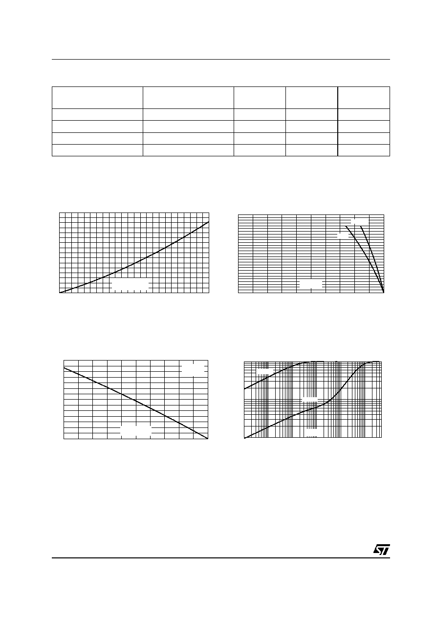
Fig. 1: Maximum power dissipation versus RMS
on-state current (full cycle).
Fig. 2-1: RMS on-state current versus case
temperature (full cycle).
Fig. 2-2: RMS on-state current versus ambient
temperature (printed circuit board FR4, copper
thickness: 35µm),full cycle.
Fig. 3: Relative variation of thermal impedance
versus pulse duration.
0
1
2
3
4
5
6
7
8
9
10
11
12
0
2
4
6
8
10
12
14
16
P (W)
IT(RMS)(A)
0
25
50
75
100
125
0
1
2
3
4
5
6
7
8
9
10
11
12
13
14
IT(RMS) (A)
BTA
BTB/T12
Tc(∞C)
0
25
50
75
100
125
0.0
0.5
1.0
1.5
2.0
2.5
3.0
3.5
Tamb(∞C)
IT(RMS) (A)
D PAK
(S=1cm )
2
2
1E-3
1E-2
1E-1
1E+0
1E+1
1E+2 5E+2
1E-2
1E-1
1E+0
K=[Zth/Rth]
Zth(j-c)
Zth(j-a)
tp(s)
BTA/BTB12 and T12 Series
5/7
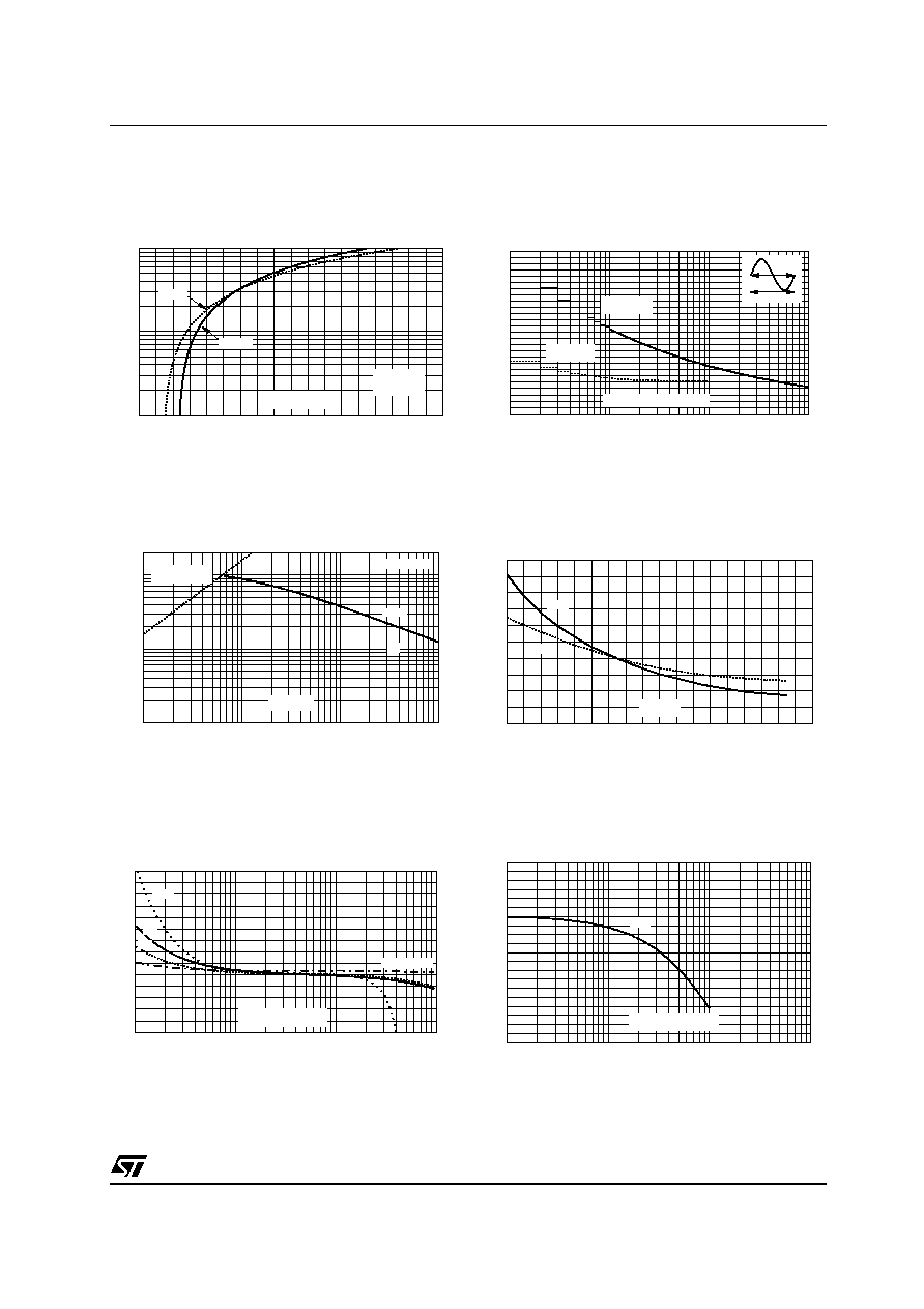
Fig. 4: On-state characteristics (maximum
values).
Fig. 5: Surge peak on-state current versus
number of cycles.
Fig. 6: Non-repetitive surge peak on-state
current for a sinusoidal pulse with width
tp < 10ms, and corresponding value of I≤t.
Fig. 7: Relative variation of gate trigger current,
holding current and latching current versus
junction temperature (typical values).
Fig. 8-1: Relative variation of critical rate of
decrease of main current versus (dV/dt)c (typical
values) (BW/CW/T1235).
Fig. 8-2: Relative variation of critical rate of
decrease of main current versus (dV/dt)c (typical
values) (TW).
0.5
1.0
1.5
2.0
2.5
3.0
3.5
4.0
4.5
5.0
1
10
100
ITM (A)
Tj=25∞C
Tj max
Tj max.
Vto = 0.85 V
Rd = 35 m
VTM(V)
1
10
100
1000
0
10
20
30
40
50
60
70
80
90
100
110
120
130
ITSM (A)
Non repetitive
Tj initial=25∞C
Repetitive
Tc=90∞C
One cycle
t=20ms
Number of cycles
0.01
0.10
1.00
10.00
10
100
1000
tp (ms)
ITSM (A), I≤t (A≤s)
Tj initial=25∞C
ITSM
I≤t
dI/dt limitation:
50A/µs
-40
-20
0
20
40
60
80
100
120
140
0.0
0.5
1.0
1.5
2.0
2.5
IGT,IH,IL[Tj] / IGT,IH,IL [Tj=25∞C]
IGT
IH & IL
Tj(∞C)
0.1
1.0
10.0
100.0
0.0
0.4
0.8
1.2
1.6
2.0
2.4
2.8
(dI/dt)c [(dV/dt)c] / Specified (dI/dt)c
BW/CW/T1235
C
B
SW
(dV/dt)c (V/µs)
0.1
5.0
4.5
4.0
3.5
3.0
2.5
2.0
1.5
1.0
0.5
0.0
1.0
10.0
100.0
(dI/dt)c [(dV/dt)c] / Specified (dI/dt)c
TW
(dV/dt)c (V/µs)