1/6
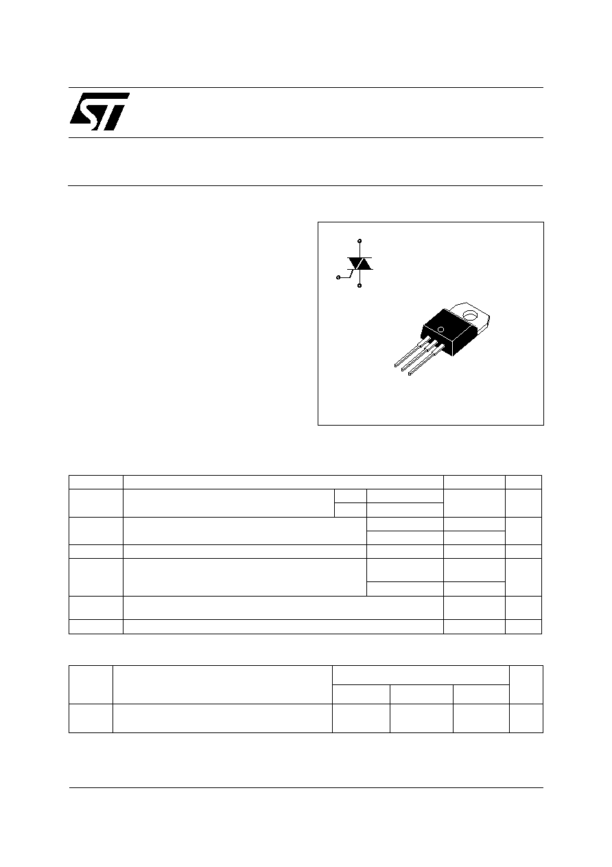
BTA04 T/D/S/A
BTB04 T/D/S/A
Æ
September 2001 - Ed: 1A
SENSITIVE GATE TRIACS
s
Very low I
GT
= 10mA max
s
Low I
H
= 15mA max
s
BTA Family:
Insulating voltage = 2500V
(RMS)
(UL recognized: E81734)
FEATURES
The BTA/BTB04 T/D/S/A triac family are high per-
formance glass passivated PNPN devices.
These parts are suitables for general purpose ap-
plications where gate high sensitivity is required.
Application on 4Q such as phase control and static
switching.
DESCRIPTION
A1
A2
G
TO-220AB
Symbol
Parameter
Value
Unit
I
T(RMS)
RMS on-state current (360∞ conduction angle)
BTA
Tc = 90∞C
4
A
BTB
Tc = 95∞C
I
TSM
Non repetitive surge peak on-state current
(Tj initial = 25∞C)
tp = 8.3ms
42
A
tp = 10ms
40
I
2
t
I
2
t value
tp = 10ms
8
A
2
s
dI/dt
Critical rate of rise of on-state current
Gate supply: I
G
= 50mA
dI
G
/dt = 0.1A/µs
Repetitive
F = 50Hz
10
A/µs
Non repetitive
50
Tstg
Tj
Storage and operating junction temperature range
-40 to +150
-40 to +110
∞C
Tl
Maximum lead soldering temperature during 10s at 4.5mm from case
260
∞C
ABSOLUTE RATINGS (limiting values)
Symbol
Parameter
BTA / BTB04-
Unit
400 T/D/S/A
600 T/D/S/A
700 T/D/S/A
V
DRM
V
RRM
Repetitive peak off-state voltage Tj = 110∞C
400
600
700
V
A1
A2
G
BTA04 T/D/S/A BTB04 T/D/S/A
2/6
Symbol
Parameter
Value
Unit
Rth (j-a)
Junction to ambient
60
∞
C/W
Rth (j-c) DC
Junction to case for DC
BTA
4.4
∞C/W
BTB
3.2
Rth (j-c) AC
Junction to case for 360∞ conduction angle (F = 50Hz)
BTA
3.3
∞C/W
BTB
2.4
GATE CHARACTERISTICS (maximum values)
P
G(AV)
= 1W
P
GM
= 40W (tp = 20µs)
I
GM
= 4A (tp = 20µs)
V
GM
= 16V (tp = 20µs)
THERMAL RESISTANCE
Symbol
Test conditions
Quadrant
BTA / BTB04
Unit
T
D
S
A
I
GT
V
D
= 12V (DC)
R
L
= 33
Tj = 25∞C
I - II - III
MAX.
5
5
10
10
mA
IV
MAX.
5
10
10
25
V
GT
V
D
= 12V (DC)
R
L
= 33
Tj = 25∞C
I - II - III - IV
MAX.
1.5
V
V
GD
V
D
= V
DRM
R
L
= 3.3k
Tj =110∞C
I - II - III - IV
MIN.
0.2
V
tgt
V
D
= V
DRM
I
G
= 40mA
dI
G
/dt = 0.5A/µs
Tj = 25∞C
I - II - III - IV
TYP.
2
µs
I
L
I
G
= 1.2I
GT
Tj = 25∞C
I - III - IV
TYP.
10
10
20
20
mA
II
20
20
40
40
I
H
*
I
T
= 100mA Gate open
Tj = 25∞C
MAX.
15
15
25
25
mA
V
TM
*
I
TM
= 5.5A
tp = 380µs
Tj = 25∞C
MAX.
1.65
V
I
DRM
I
RRM
V
DRM
rated
V
RRM
rated
Tj = 25∞C
MAX.
0.01
mA
Tj = 110∞C
MAX.
0.75
dV/dt *
Linear slope up to
V
D
= 67% V
DRM
gate open
Tj = 110∞C
TYP.
10
10
-
-
V/
µ
s
MIN.
-
-
10
10
(dI/dt)c*
(dI/dt)c = 1.8A/ms
Tj = 110∞C
TYP.
1
1
5
5
V/µs
* For either polarity of electrode A
2
voltage with reference to electrode A
1
ELECTRICAL CHARACTERISTICS
BTA04 T/D/S/A BTB04 T/D/S/A
3/6
Package
I
T(RMS)
V
DRM
/ V
RRM
Sensitivity Specification
A
V
T
D
S
A
BTA
(Insulated)
4
400
X
X
600
X
X
700
X
X
BTB
(Uninsulated)
400
X
X
600
X
X
PRODUCT INFORMATION
BT A 04 - 400
T
Triac
Series
Insulation:
A: insulated
B: non insulated
Current: 04A
Voltage:
400: 400V
600: 600V
700: 700V
Sensitivity
ORDERING INFORMATION
BTA04 T/D/S/A BTB04 T/D/S/A
4/6
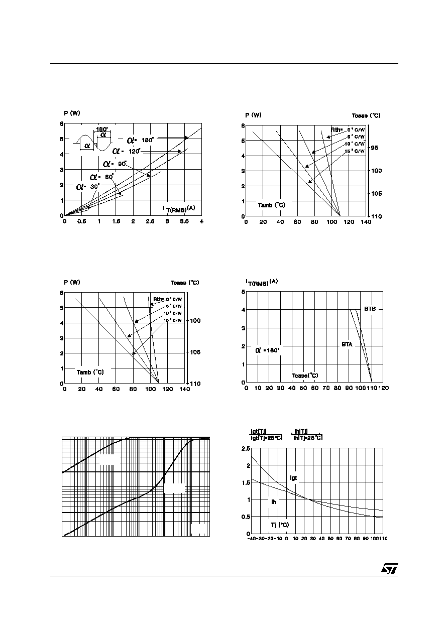
Fig. 3: Correlation between maximum RMS power
dissipation and maximum allowable temperature
(Tamb and Tcase) for different thermal resistances
heatsink + contact (BTB).
Fig. 4: RMS on-state current versus case temper-
ature.
1E-3
1E-2
1E-1
1E+0
1E+1
1E +2 5E+2
0.01
0.1
1
Zth/Rth
Zth(j-c)
Zth(j-a)
tp(s)
Fig. 5: Relative variation of thermal impedance
versus pulse duration.
Fig. 6: Relative variation of gate trigger current
and holding current versus junction temperature.
Fig. 1: Maximum RMS power dissipation versus
RMS on-state current (F = 50Hz).(Curves are cut
off by (dI/dt)c limitation)
Fig. 2: Correlation between maximum RMS power
dissipation and maximum allowable temperature
(Tamb and Tcase) for different thermal resistances
heatsink + contact (BTA).
BTA04 T/D/S/A BTB04 T/D/S/A
5/6
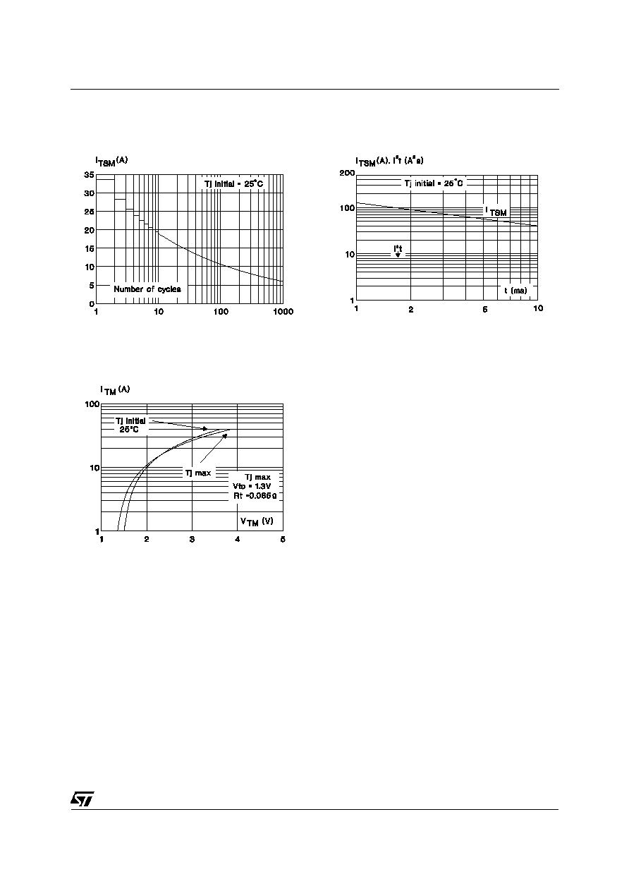
Fig. 9: On-state characteristics (maximum values).
Fig. 7: Non repetitive surge peak on-state current
versus number of cycles.
Fig. 8: Non repetitive surge peak on-state current
for a sinusoidal pulse with width: t
10ms, and cor-
responding value of I
2
t.