1/5
BTW67 and BTW69 Series
STANDARD
50A SCRs
April 2001 - Ed: 4
MAIN FEATURES:
DESCRIPTION
Available in high power packages, the BTW67 /
BTW69 Series is suitable in applications where
power handling and power dissipation are critical,
such as solid state relays, welding equipment,
high power motor control.
Based on a clip assembly technology, they offer a
superior performance in surge current handling
capabilities.
Thanks to their internal ceramic pad, they provide
high voltage insulation (2500V RMS), complying
with UL standards (file ref: E81734).
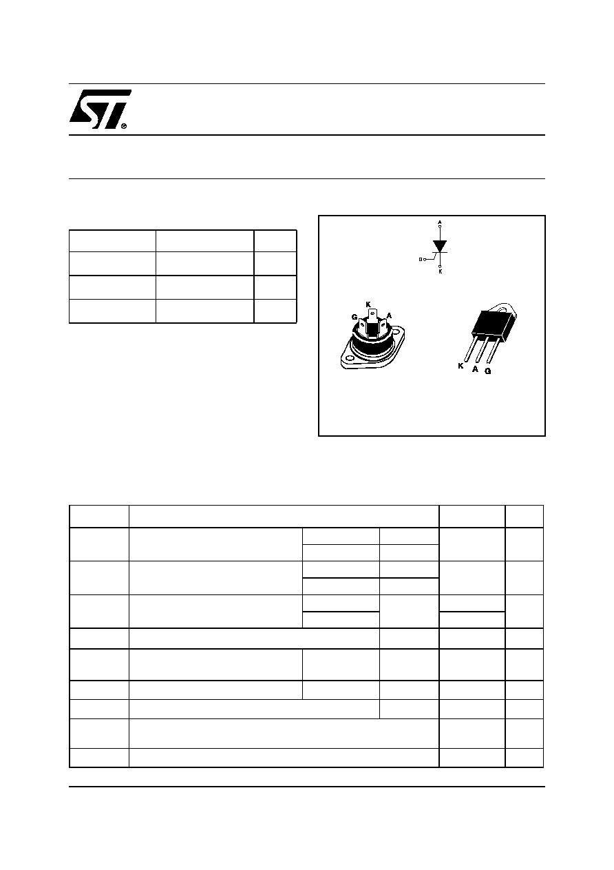
Symbol
Value
Unit
I
T(RMS)
50
A
V
DRM
/V
RRM
600 to 1200
V
I
GT
80
mA
ABSOLUTE RATINGS (limiting values)
Symbol
Parameter
Value
Unit
I
T(RMS)
RMS on-state current
(180∞ conduction angle)
RD91
Tc = 70∞C
50
A
TOP3 Ins.
Tc = 75∞C
I
T(AV)
Average on-state current
(180∞ conduction angle)
RD91
Tc = 70∞C
32
A
TOP3 Ins.
Tc = 75∞C
I
TSM
Non repetitive surge peak on-state current
tp = 8.3 ms
Tj = 25∞C
610
A
tp = 10 ms
580
I
≤
t
I
≤
t Value for fusing
Tj = 25∞C
1680
A
2
S
dI/dt
Critical rate of rise of on-state current I
G
=
2 x I
GT
, tr
100 ns
F = 60 Hz
Tj = 125∞C
50
A/µs
I
GM
Peak gate current
tp = 20 µs
Tj = 125∞C
8
A
P
G(AV)
Average gate power dissipation
Tj = 125∞C
1
W
T
stg
Tj
Storage junction temperature range
Operating junction temperature range
- 40 to + 150
- 40 to + 125
∞C
V
RGM
Maximum peak reverse gate voltage
5
V
RD91
(BTW67)
TOP3
(BTW69)
BTW67 and BTW69 Series
3/5
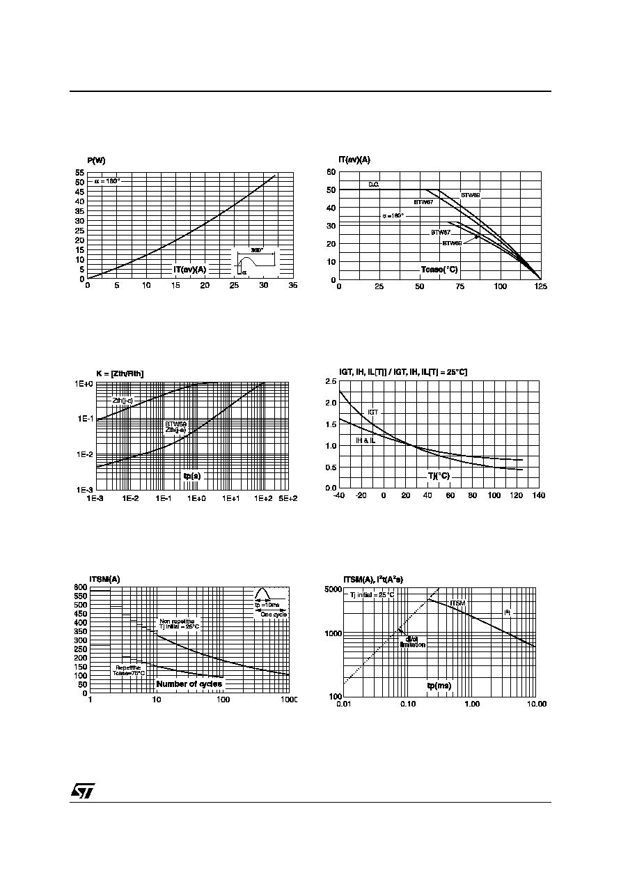
Fig. 1: Maximum average power dissipation
versus average on-state current.
Fig. 2: Average and D.C. on-state current versus
case temperature.
Fig. 3: Relative variation of thermal impedance
versus pulse duration.
Fig. 4: Relative variation of gate trigger current,
holding current and latching current versus
junction temperature.
Fig. 5:
Surge peak on-state current versus
number of cycles.
Fig. 6:
Non-repetitive surge
peak on-state
current
for
a
sinusoidal
pulse
with
width
tp < 10ms, and corresponding value of I≤t.
BTW67 and BTW69 Series
5/5
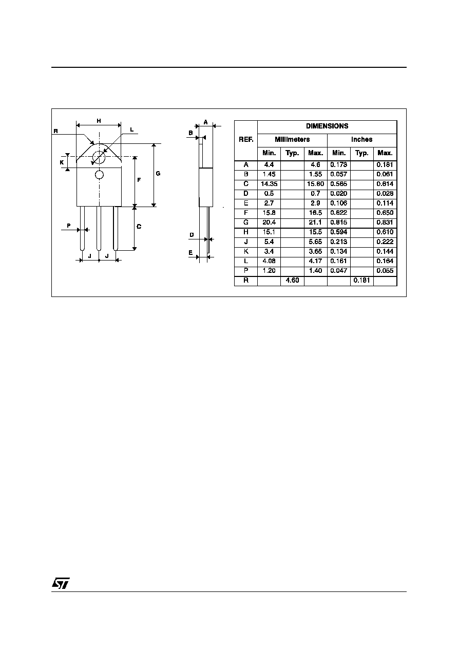
PACKAGE MECHANICAL DATA
TOP3 Ins.(Plastic)
Information furnished is believed to be accurate and reliable. However, STMicroelectronics assumes no responsibility for
the consequences of use of such information nor for any infringement of patents or other rights of third parties which may
result from its use. No license is granted by implication or otherwise under any patent or patent rights of
STMicroelectronics. Specifications mentioned in this publication are subject to change without notice. This publication
supersedes and replaces all information previously supplied.STMicroelectronics products are not authorized for use as
critical components in life support devices or systems without express written approval of STMicroelectronics.
© The ST logo is a registered trademark of STMicroelectronics
© 2001 STMicroelectronics - Printed in Italy - All rights reserved
.
STMicroelectronics GROUP OF COMPANIES
Australia - Brazil - China - Finland - France - Germany - Hong Kong - India - Italy - Japan - Malaysia-Malta - Morocco
Singapore - Spain - Sweden - Switzerland - United Kingdom - U.S.A.
http://www.st.com

