 | –≠–ª–µ–∫—Ç—Ä–æ–Ω–Ω—ã–π –∫–æ–º–ø–æ–Ω–µ–Ω—Ç: BU808DFH | –°–∫–∞—á–∞—Ç—å:  PDF PDF  ZIP ZIP |
BU808DFH
HIGH VOLTAGE FAST-SWITCHING
NPN POWER DARLINGTON TRANSISTOR
s
NEW Fully Plastic TO-220 for HIGH
VOLTAGE APPLICATIONS
s
NPN MONOLITHIC DARLINGTON WITH
INTEGRATED FREE-WHEELING DIODE
s
HIGH VOLTAGE CAPABILITY ( > 1400 V )
s
HIGH DC CURRENT GAIN ( TYP. 150 )
s
LOW BASE-DRIVE REQUIREMENTS
s
DEDICATED APPLICATION NOTE AN1184
s
FULLY INSULATED PACKAGE (U.L.
COMPLIANT) FOR EASY MOUNTING
s
CREEPAGE PATH > 4 mm
APPLICATIONS
s
COST EFFECTIVE SOLUTION FOR
HORIZONTAL DEFLECTION IN LOW END
TV UP TO 21 INCHES.
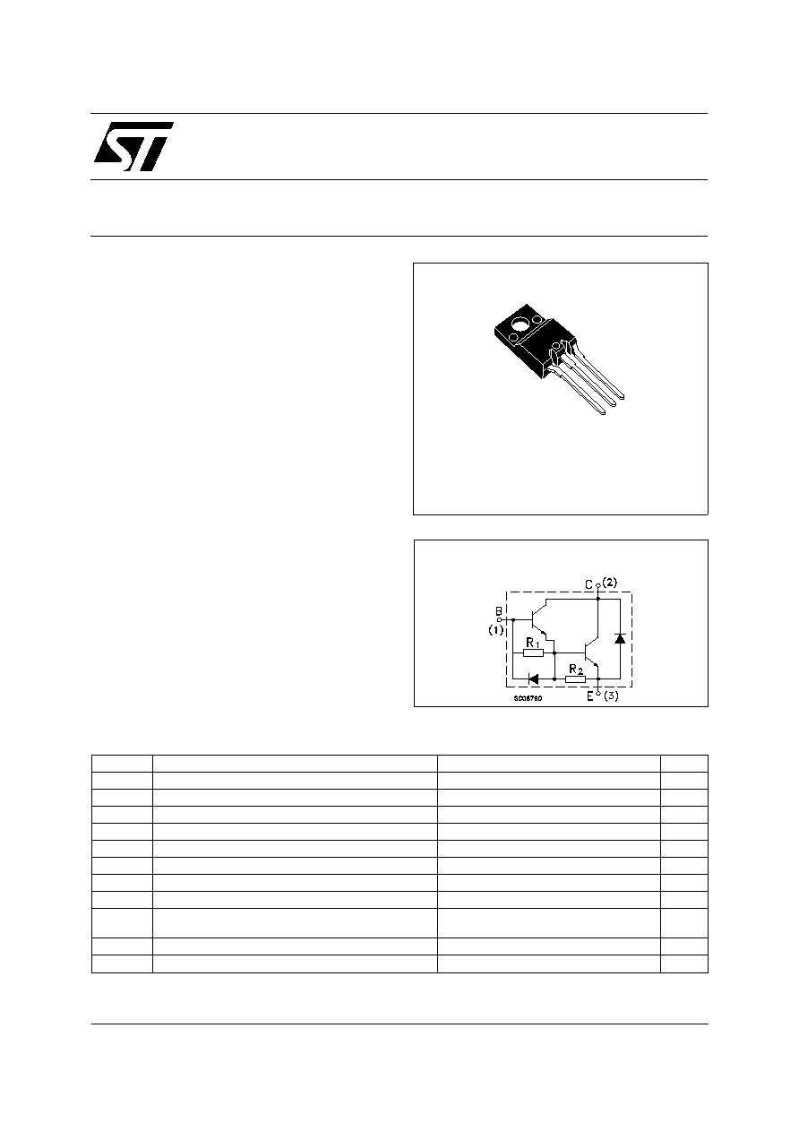
DESCRIPTION
The BU808DFH is a NPN transistor in monolithic
Darlington configuration. It is manufactured using
Multiepitaxial Mesa technology for cost-effective
high performance.
Æ
INTERNAL SCHEMATIC DIAGRAM
April 2002
ABSOLUTE MAXIMUM RATINGS
Symbol
Parameter
Value
Unit
V
CBO
Collector-Base Voltage (I
E
= 0)
1400
V
V
CEO
Collector-Emitter Voltage (I
B
= 0)
700
V
V
EBO
Emitter-Base Voltage (I
C
= 0)
5
V
I
C
Collector Current
8
A
I
CM
Collector Peak Current (t
p
< 5 ms)
10
A
I
B
Base Current
3
A
I
BM
Base Peak Current (t
p
< 5 ms)
6
A
P
tot
Total Dissipation at T
c
= 25
o
C
42
W
V
isol
Insulation Withstand Voltage (RMS) from All
Three Leads to Exernal Heatsink
2500
V
T
stg
Storage Temperature
-65 to 150
o
C
T
j
Max. Operating Junction Temperature
150
o
C
TO-220FH
(see page 6)
1/7
THERMAL DATA
R
thj-case
Thermal Resistance Junction-case Max
2.98
o
C/W
ELECTRICAL CHARACTERISTICS (T
case
= 25
o
C unless otherwise specified)
Symbol
Parameter
Test Conditions
Min.
Typ.
Max.
Unit
I
CES
Collector Cut-off
Current (V
BE
= 0)
V
CE
= 1400 V
400
µ
A
I
EBO
Emitter Cut-off Current
(I
C
= 0)
V
EB
= 5 V
100
mA
V
CE(sat)
Collector-Emitter
Saturation Voltage
I
C
= 5 A I
B
= 0.5 A
1.6
V
V
BE(sat)
Base-Emitter
Saturation Voltage
I
C
= 5 A I
B
= 0.5 A
2.1
V
h
FE
DC Current Gain
I
C
= 5 A V
CE
= 5 V
I
C
= 5 A V
CE
= 5 V T
C
= 100
o
C
60
20
230
t
s
t
f
INDUCTIVE LOAD
Storage Time
Fall Time
V
CC
= 150 V I
C
= 5 A
I
B1
= 0.5 A V
BE(o ff)
= -5 V
3
0.8
µ
s
µ
s
t
s
t
f
INDUCTIVE LOAD
Storage Time
Fall Time
V
CC
= 150 V I
C
= 5 A
I
B1
= 0.5 A V
BE(o ff)
= -5 V
T
C
= 100
o
C
2
0.8
µ
s
µ
s
V
F
Diode Forward Voltage
I
F
= 5 A
3
V
Pulsed: Pulse duration = 300
µ
s, duty cycle 1.5 %
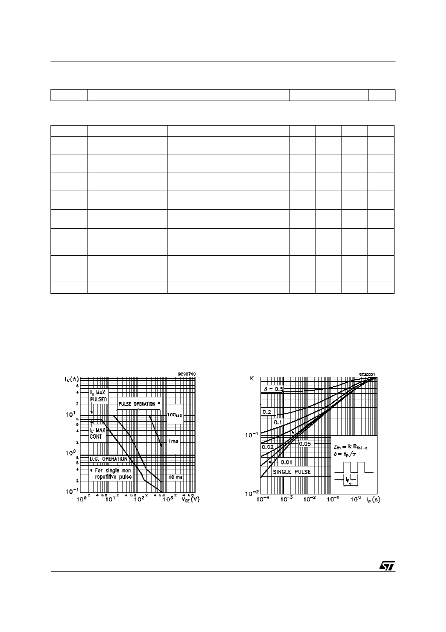
Safe Operating Area
Thermal Impedance
BU808DFH
2/7
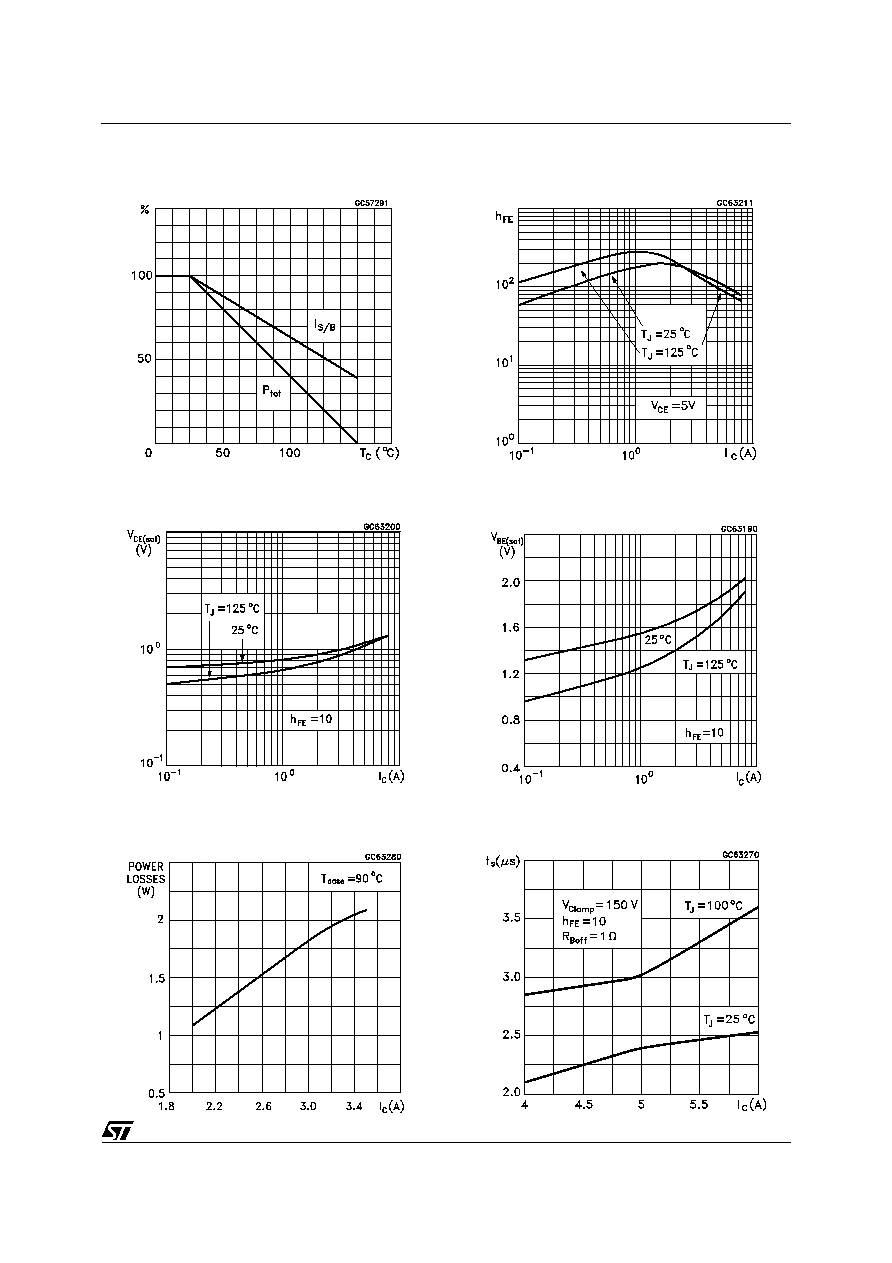
Derating Curve
Collector Emitter Saturation Voltage
Power Losses at 16 KHz
DC Current Gain
Base Emitter Saturation Voltage
Switching Time Inductive Load at 16KHz
BU808DFH
3/7

Switching Time Inductive Load at 16KHZ
Reverse Biased SOA
BASE DRIVE INFORMATION
In order to saturate the power switch and reduce
conduction losses, adequate direct base current
I
B1
has to be provided for the lowest gain h
FE
at
100
o
C (line scan phase). On the other hand,
negative base current I
B2
must be provided to
turn off the power transistor (retrace phase).
Most of the dissipation, in the deflection
application, occurs at switch-off. Therefore it is
essential to determine the value of I
B2
which
minimizes power losses, fall time t
f
and,
consequently, T
j
. A new set of curves have been
defined to give total power losses, t
s
and t
f
as a
function of I
B2
at both 16 KHz scanning
frequencies for choosing the optimum negative
drive. The test circuit is illustrated in figure 1.
Inductance L
1
serves to control the slope of the
negative base current I
B2
to recombine the
excess carrier in the collector when base current
is still present, this would avoid any tailing
phenomenon in the collector current.
The values of L and C are calculated from the
following equations:
1
2
L
(
I
C
)
2
=
1
2
C
(
V
CEfly
)
2
=
2
f
=
1
L
C
Where I
C
= operating collector current, V
CEfly
=
flyback voltage, f= frequency of oscillation during
retrace.
BU808DFH
4/7

Figure 1: Inductive Load Switching Test Circuits.
Figure 2: Switching Waveforms in a Deflection Circuit
BU808DFH
5/7
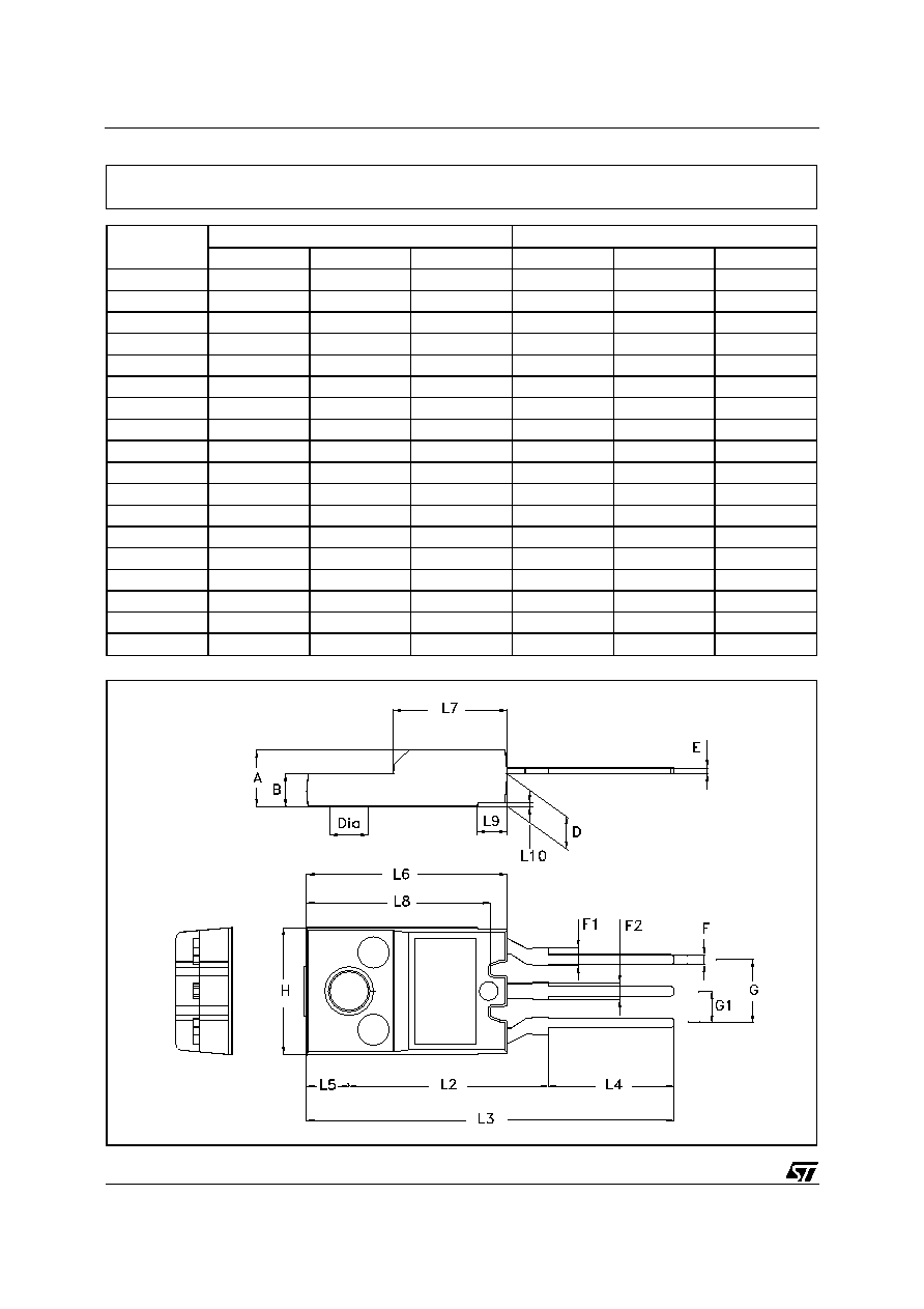
DIM.
mm
inch
MIN.
TYP.
MAX.
MIN.
TYP.
MAX.
A
4.4
4.6
0.173
0.181
B
2.5
2.7
0.098
0.106
D
2.5
2.75
0.098
0.108
E
0.45
0.7
0.017
0.027
F
0.75
1
0.030
0.039
F1
1.3
1.8
0.051
0.070
F2
1.3
1.8
0.051
0.070
G
4.95
5.2
0.195
0.204
G1
2.4
2.7
0.094
0.106
H
10
10.4
0.393
0.409
L2
16
0.630
L3
28.6
30.6
1.126
1.204
L4
9.8
10.6
0.385
0.417
L5
3.4
0.134
L6
15.9
16.4
0.626
0.645
L7
9
9.3
0.354
0.366
L8
14.5
15
0.570
0.590
L9
2.4
0.094
P011W
TO-220FH (Fully plastic High voltage) MECHANICAL DATA
BU808DFH
6/7

Information furnished is believed to be accurate and reliable. However, STMicroelectronics assumes no responsibility for the consequences
of use of such information nor for any infringement of patents or other rights of third parties which may result from its use. No license is
granted by implication or otherwise under any patent or patent rights of STMicroelectronics. Specification mentioned in this publication are
subject to change without notice. This publication supersedes and replaces all information previously supplied. STMicroelectronics products
are not authorized for use as critical components in life support devices or systems without express written approval of STMicroelectronics.
The ST logo is a trademark of STMicroelectronics
© 2002 STMicroelectronics ≠ Printed in Italy ≠ All Rights Reserved
STMicroelectronics GROUP OF COMPANIES
Australia - Brazil - Canada - China - Finland - France - Germany - Hong Kong - India - Israel - Italy - Japan - Malaysia - Malta - Morocco -
Singapore - Spain - Sweden - Switzerland - United Kingdom - United States.
http://www.st.com
BU808DFH
7/7