
BUH313
HIGH VOLTAGE FASTSWITCHING NPN
POWER TRANSISTOR
s
SGS-THOMSON PREFERRED SALESTYPE
s
HIGH VOLTAGE CAPABILITY
s
U.L. RECOGNISED ISOWATT218 PACKAGE
(U.L. FILE # E81734 (N)).
APPLICATIONS:
s
HORIZONTAL DEFLECTION FOR COLOUR
TV
s
SWITCH MODE POWER SUPPLIES
DESCRIPTION
The BUH313 is manufactured using Multiepitaxial
Mesa
technology
for
cost-effective
high
performance and uses a Hollow Emitter structure
to enhance switching speeds.
The BUH series is designed for use in horizontal
deflection circuits in televisions and monitors.
INTERNAL SCHEMATIC DIAGRAM
June 1996
ABSOLUTE MAXIMUM RATINGS
Symb ol
Parameter
Valu e
Unit
V
CBO
Collector-Base Voltage (I
E
= 0)
1300
V
V
CEO
Collector-Emit ter Voltage (I
B
= 0)
600
V
V
EBO
Emitter-Base Voltage (I
C
= 0)
10
V
I
C
Collector Current
5
A
I
CM
Collector Peak Current (t
p
< 5 ms)
8
A
I
B
Base Current
3
A
I
BM
Base Peak Current (t
p
< 5 ms)
5
A
P
tot
T otal Dissipat ion at T
c
= 25
o
C
44
W
T
s tg
Storage Temperat ure
-65 to 150
o
C
T
j
Max. O perat ing Junction Temperature
150
o
C
1
2
3
ISOWATT218
1/7

THERMAL DATA
R
thj -ca se
Thermal Resistance Junction-case
Max
2.8
o
C/W
ELECTRICAL CHARACTERISTICS (T
case
= 25
o
C unless otherwise specified)
Symbo l
Parameter
T est Con ditio ns
Min .
T yp.
Max.
Uni t
I
CES
Collector Cut -off
Current (V
BE
= 0)
V
CE
= 1300 V
V
CE
= 1300 V
T
j
= 125
o
C
1
2
mA
mA
I
EBO
Emitter Cut- off Current
(I
C
= 0)
V
EB
= 5 V
100
�
A
V
CEO(s us)
Collector-Emitt er
Sustaining Voltage
I
C
= 100 mA
600
V
V
EBO
Emitter-Base Voltage
(I
C
= 0)
I
E
= 10 mA
10
V
V
CE(sat)
Collector-Emitt er
Sat uration Voltage
I
C
= 3 A
I
B
= 0.75 A
1.5
V
V
BE(sat )
Base-Emitter
Sat uration Voltage
I
C
= 3 A
I
B
= 0.75 A
1.3
V
h
FE
DC Current Gain
I
C
= 3 A
V
CE
= 5 V
I
C
= 3 A
V
CE
= 5 V
T
j
= 100
o
C
5.5
3.5
t
s
t
f
RESISTIVE LOAD
Storage Time
Fall Time
V
CC
= 400 V
I
C
= 3 A
I
B1
= 0.75 A
I
B2
= 1.5 A
1. 6
110
2.4
200
�
s
ns
t
s
t
f
INDUCT IVE LOAD
Storage Time
Fall Time
I
C
= 3 A
f = 15625 Hz
I
B1
= 0.75 A
I
B2
= -1.5 A
V
cef ly back
= 1050 sin
5
10
6
t
V
3. 5
340
�
s
ns
t
s
t
f
INDUCT IVE LOAD
Storage Time
Fall Time
I
C
= 3 A
f = 31250 Hz
I
B1
= 0.75 A
I
B2
= -1.5 A
V
cef ly back
= 1200 sin
5
10
6
t
V
3. 5
270
�
s
ns
Pulsed: Pulse duration = 300
�
s, duty cycle 1.5 %
Safe Operating Area
Thermal Impedance
BUH313
2/7

Derating Curve
Collector Emitter Saturation Voltage
Power Losses at 16 KHz
DC Current Gain
Base Emitter Saturation Voltage
Switching Time Inductive Load at 16KHz
(see figure 2)
BUH313
3/7
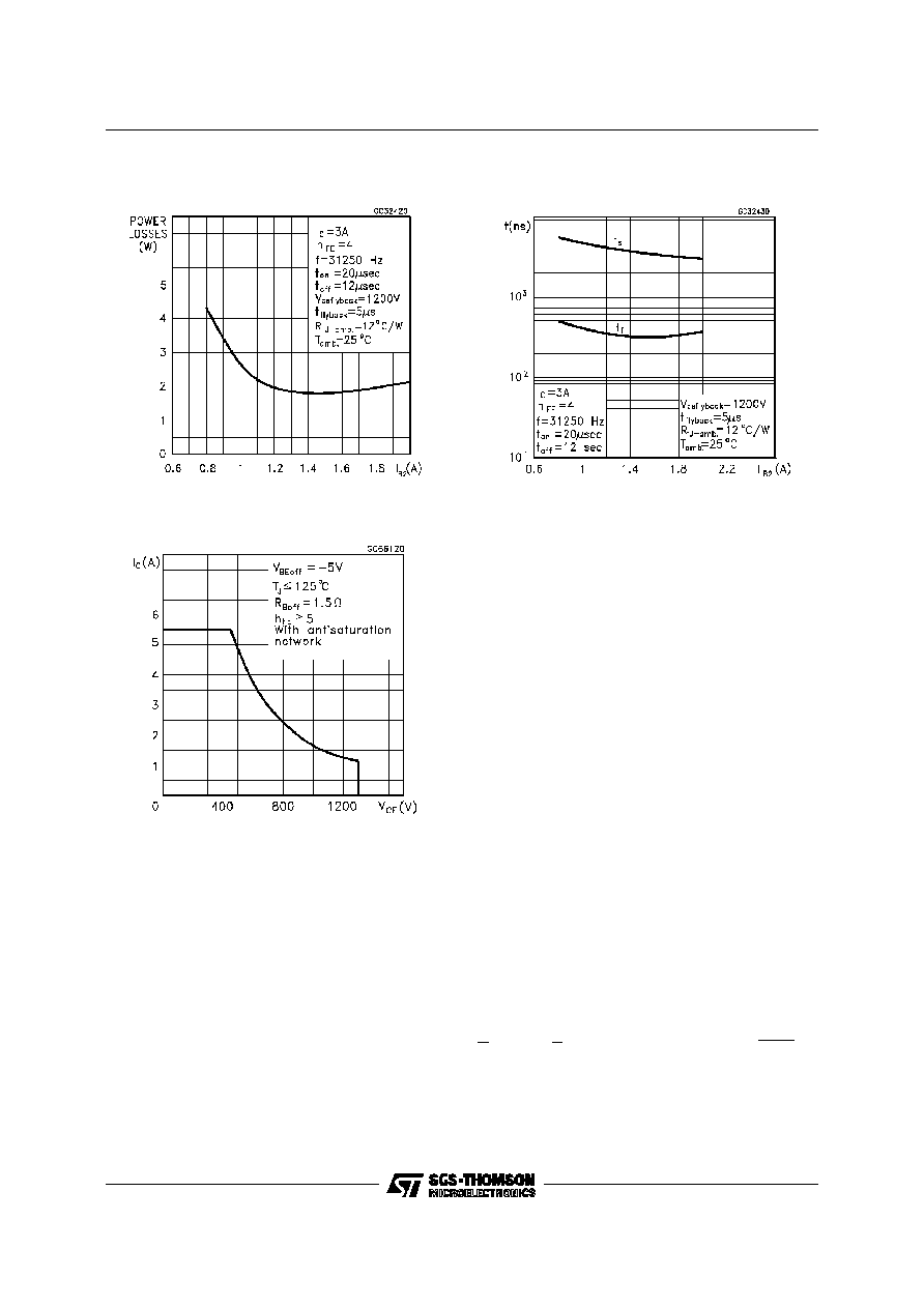
Power Losses at 32 KHz
Switching Time Inductive Load at 32 KHz
(see figure 2)
In order to saturate the power switch and reduce
conduction losses, adequate direct base current
I
B1
has to be provided for the lowest gain h
FE
at
100
o
C (line scan phase). On the other hand,
negative base current I
B2
must be provided to
turn off the power transistor (retrace phase).
Most
of
the
dissipation,
in
the
deflection
application, occurs at switch-off. Therefore it is
essential to determine the value of I
B2
which
minimizes
power
losses,
fall
time
t
f
and,
consequently, T
j
. A new set of curves have been
defined to give total power losses, t
s
and t
f
as a
function of I
B2
at both 16 KHz,
32 KHz and
64KHz scanning frequencies for choosing the
optimum negative drive. The test circuit is
illustrated in figure 1.
Inductance L
1
serves to control the slope of the
negative base current I
B2
to recombine the
excess carrier in the collector when base current
is still present, this would avoid any tailing
phenomenon in the collector current.
The values of L and C are calculated from the
following equations:
1
2
L
(
I
C
)
2
=
1
2
C
(
V
CEfly
)
2
=
2
f
=
1
L
C
Where I
C
= operating collector current, V
CEfly
=
flyback voltage, f= frequency of oscillation during
retrace.
BASE DRIVE INFORMATION
Reverse Biased SOA
BUH313
4/7

Figure 1: Inductive Load Switching Test Circuits.
Figure 2: Switching Waveforms in a Deflection Circuit
BUH313
5/7