 | –≠–ª–µ–∫—Ç—Ä–æ–Ω–Ω—ã–π –∫–æ–º–ø–æ–Ω–µ–Ω—Ç: BUH315 | –°–∫–∞—á–∞—Ç—å:  PDF PDF  ZIP ZIP |
BUH315
HIGH VOLTAGE FAST-SWITCHING
NPN POWER TRANSISTOR
s
STMicroelectronics PREFERRED
SALESTYPE
s
HIGH VOLTAGE CAPABILITY
s
U.L. RECOGNISED ISOWATT218 PACKAGE
(U.L. FILE # E81734 (N)).
APPLICATIONS:
s
HORIZONTAL DEFLECTION FOR COLOUR
TV
s
SWITCH MODE POWER SUPPLIES
DESCRIPTION
The BUH315 is manufactured using Multiepitaxial
Mesa
technology
for
cost-effective
high
performance and uses a Hollow Emitter structure
to enhance switching speeds.
The BUH series is designed for use in horizontal
deflection circuits in televisions and monitors.
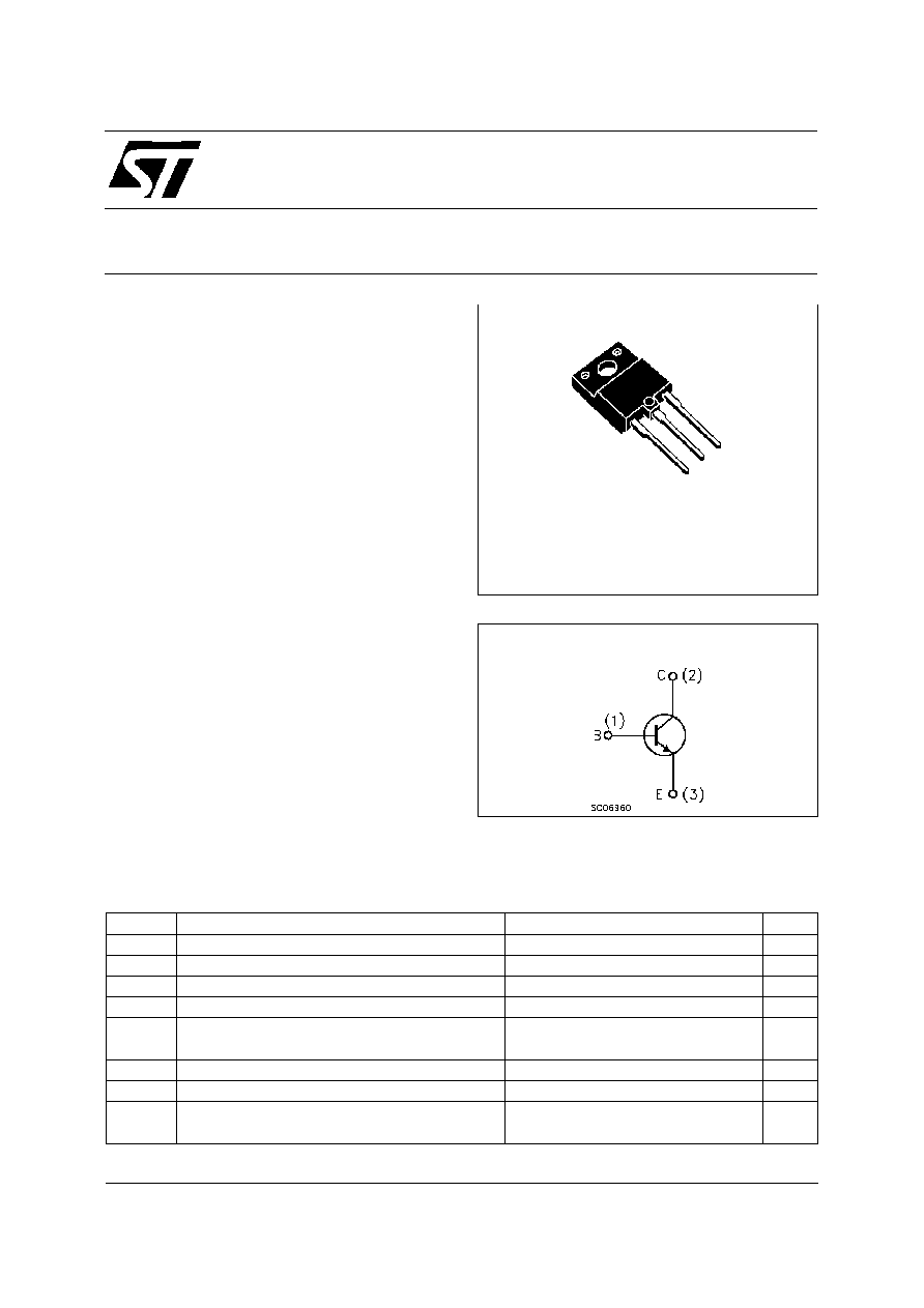
Æ
INTERNAL SCHEMATIC DIAGRAM
November 1999
ABSOLUTE MAXIMUM RATINGS
Symbol
Parameter
Val ue
Uni t
V
CBO
Collector-Base Voltage (I
E
= 0)
1500
V
V
CEO
Collector-Emit ter Volt age (I
B
= 0)
700
V
V
EBO
Emitt er-Base Voltage (I
C
= 0)
10
V
I
C
Collector Current
6
A
I
CM
Collector Peak Current (t
p
< 5 ms)
12
A
I
B
Base Current
3
A
I
BM
Base Peak Current (t
p
< 5 ms)
5
A
P
t ot
Tot al Dissipation at T
c
= 25
o
C
44
W
T
stg
St orage Temperature
-65 to 150
o
C
T
j
Max. Operat ing Junction Temperat ure
150
o
C
1
2
3
ISOWATT218
1/7
THERMAL DATA
R
t hj-ca se
Thermal Resistance Junction-case
Max
2.8
o
C/W
ELECTRICAL CHARACTERISTICS (T
case
= 25
o
C unless otherwise specified)
Symb ol
Parameter
Test Cond ition s
Mi n.
Typ .
Max.
Un it
I
CES
Collector Cut -of f
Current (V
BE
= 0)
V
CE
= 1500 V
200
µ
A
I
EBO
Emitt er Cut -of f Current
(I
C
= 0)
V
EB
= 5 V
100
µ
A
V
CEO(sus )
Collector-Emit ter
Sustaining Voltage
(I
B
= 0)
I
C
= 100 mA
700
V
V
EBO
Emitt er-Base Voltage
(I
C
= 0)
I
E
= 10 mA
10
V
V
CE(sat )
Collector-Emit ter
Saturation Voltage
I
C
= 3 A
I
B
= 0.75 A
1.5
V
V
BE(s at)
Base-Emitt er
Saturation Voltage
I
C
= 3 A
I
B
= 0.75 A
1.3
V
h
F E
DC Current Gain
I
C
= 3 A
V
CE
= 5 V
I
C
= 3 A
V
CE
= 5 V
T
j
= 100
o
C
6
3. 5
12
t
s
t
f
RESI STIVE LO AD
St orage Time
Fall Time
V
CC
= 400 V
I
C
= 3 A
I
B1
= 0.75 A
I
B2
= 1.5 A
1.6
110
2.4
200
µ
s
ns
t
s
t
f
INDUCTIVE LO AD
St orage Time
Fall Time
I
C
= 3 A
f = 15625 Hz
I
B1
= 0.75 A
I
B2
= -1.5 A
V
c eflybac k
= 1050 sin
5
10
6
t
V
3.5
340
µ
s
ns
t
s
t
f
INDUCTIVE LO AD
St orage Time
Fall Time
I
C
= 3 A
f = 31250 Hz
I
B1
= 0.75 A
I
B2
= -1.5 A
V
c eflybac k
= 1200 sin
5
10
6
t
V
3.5
270
µ
s
ns
Pulsed: Pulse duration = 300
µ
s, duty cycle 1.5 %
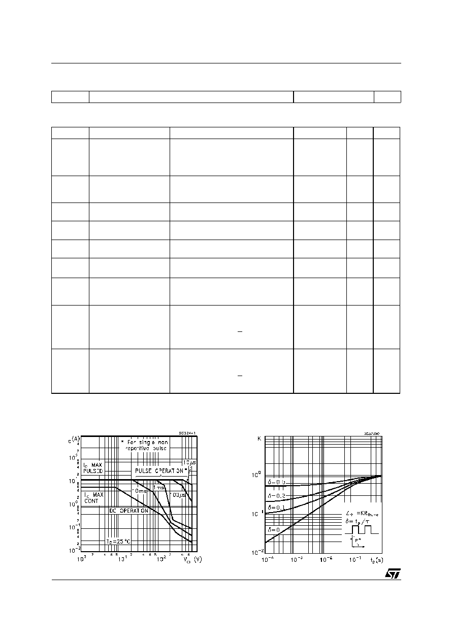
Safe Operating Area
Thermal Impedance
BUH315
2/7

Derating Curve
Collector Emitter Saturation Voltage
Power Losses at 16 KHz
DC Current Gain
Base Emitter Saturation Voltage
Switching Time Inductive Load at 16KHz
(see figure 2)
BUH315
3/7

Power Losses at 32 KHz
Switching Time Inductive Load at 32 KHz
(see figure 2)
In order to saturate the power switch and reduce
conduction losses, adequate direct base current
I
B1
has to be provided for the lowest gain h
FE
at
100
o
C (line scan phase). On the other hand,
negative base current I
B2
must be provided to
turn off the power transistor (retrace phase).
Most
of
the
dissipation,
in
the
deflection
application, occurs at switch-off. Therefore it is
essential to determine the value of I
B2
which
minimizes
power
losses,
fall
time
t
f
and,
consequently, T
j
. A new set of curves have been
defined to give total power losses, t
s
and t
f
as a
function of I
B2
at both 16 KHz and 32 KHz
scanning frequencies for choosing the optimum
negative drive. The test circuit is illustrated in
figure 1.
Inductance L
1
serves to control the slope of the
negative base current I
B2
to recombine the
excess carrier in the collector when base current
is still present, this would avoid any tailing
phenomenon in the collector current.
The values of L and C are calculated from the
following equations:
1
2
L
(
I
C
)
2
=
1
2
C
(
V
CEfly
)
2
=
2
f
=
1
L
C
Where I
C
= operating collector current, V
CEfly
=
flyback voltage, f= frequency of oscillation during
retrace.
BASE DRIVE INFORMATION
Reverse Biased SOA
BUH315
4/7
Figure 1: Inductive Load Switching Test Circuits.
Figure 2: Switching Waveforms in a Deflection Circuit
BUH315
5/7