
1/6
August 2002
BUL312FH
HIGH VOLTAGE FAST-SWITCHING
NPN POWER TRANSISTOR
HIGH VOLTAGE CAPABILITY
LOW SPREAD OF DYNAMIC PARAMETERS
MINIMUM LOT-TO-LOT SPREAD FOR
RELIABLE OPERATION
VERY HIGH SWITCHING SPEED
FULLY CHARACTERIZED AT 125 ∞C
LARGE R.B.S.O.A.
FULLY INSULATED PACKAGE (U.L.
COMPLIANT) FOR EASY MOUNTING
APPLICATIONS:
HORIZONTAL DEFLECTION FOR COLOR TV
SWITCH MODE POWER SUPPLIES
ELECTRONIC BALLASTS FOR
FLUORESCENT LIGHTING
DESCRIPTION
The device is manufactured using High Voltage
Multi Epitaxial Planar technology for high switching
speeds and high voltage capability.
It uses a Cellular Emitter structure with planar edge
termination to enhance switching speeds while
maintaining a wide R.B.S.O.A.
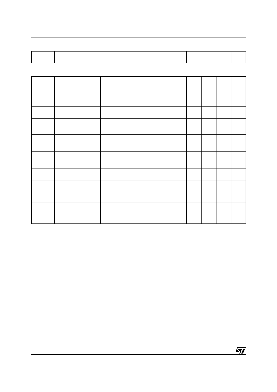
ABSOLUTE MAXIMUM RATINGS
Ordering Code
Marking
Shipment
BUL312FH
BUL312FH
Tube
Symbol
Parameter
Value
Unit
V
CES
Collector-Emitter Voltage (V
BE
= 0)
1150
V
V
CEO
Collector-Emitter Voltage (I
B
= 0)
500
V
V
EBO
Emitter-Base Voltage (I
C
= 0)
9
V
I
C
Collector Current
5
A
I
CM
Collector Peak Current (t
p
< 5 ms)
10
A
I
B
Base Current
3
A
I
BM
Base Peak Current (t
p
< 5 ms)
4
A
P
tot
Total Dissipation at T
c
= 25 ∞C
36
W
V
isol
Insulation Withstand Voltage (RMS) from All Three
Leads to External Heatsink
2500
V
T
stg
Storage Temperature
≠65 to 150
∞C
T
j
Max. Operating Junction Temperature
150
∞C
TO-220FH
INTERNAL SCHEMATIC DIAGRAM
BUL312FH
2/6
THERMAL DATA
ELECTRICAL CHARACTERISTICS (T
j
= 25 ∞C unless otherwise specified)
* Pulsed: Pulse duration = 300 µs, duty cycle = 1.5 %.
R
thj-case
R
thj-amb
Thermal Resistance Junction-case
Thermal Resistance Junction-ambient
Max
Max
3.47
62.5
∞C/W
∞C/W
Symbol
Parameter
Test Conditions
Min.
Typ.
Max.
Unit
I
CES
Collector Cut-off
Current (V
BE
= 0)
V
CE
= 1150 V
V
CE
= 1150 V
T
j
= 125 ∞C
1
2
mA
mA
I
CEO
Collector Cut-off
Current (I
B
= 0)
V
CE
= 500 V
250
µ
A
V
EBO
Emitter-Base Voltage
(I
C
= 0)
I
E
= 10 mA
9
V
V
CEO(sus)
*
Collector-Emitter
Sustaining Voltage
(I
B
= 0)
I
C
= 100 mA
500
V
V
CE(sat)
*
Collector-Emitter
Saturation Voltage
I
C
= 1 A
I
C
= 2 A
I
C
= 3 A
I
B
= 200 mA
I
B
= 400 mA
I
B
= 600 mA
0.5
0.7
1.1
V
V
V
V
BE(sat)
*
Base-Emitter
Saturation Voltage
I
C
= 1 A
I
C
= 2 A
I
C
= 3 A
I
B
= 200 mA
I
B
= 400 mA
I
B
= 600 mA
1
1.1
1.2
V
V
V
h
FE
*
DC Current Gain
I
C
= 10 mA
I
C
= 3 A
V
CE
= 5 V
V
CE
= 2.5 V
8
8
16
t
s
t
f
INDUCTIVE LOAD
Storage Time
Fall Time
I
C
= 2 A
I
B1
= 400 mA
L = 200 µH
(See Figure 1)
V
clamp
= 250 V
V
BE(off)
= -5 V
R
BB
= 0
1.2
80
1.9
160
µs
ns
t
s
t
f
INDUCTIVE LOAD
Storage Time
Fall Time
I
C
= 2 A
I
B1
= 400 mA
L = 200 µH
T
j
= 125 ∞C
V
clamp
= 250 V
V
BE(off)
= -5 V
R
BB
= 0
(See Figure 1)
1.8
150
µs
ns

BUL312FH
4/6
Figure 1: Inductive Load Switching Test Circuit
1) Fast Electronic Switch
2) Non-Inductive Resistor
3) Fast Recovery Rectifier
Inductive Load Storage Time
Reverse Biased Safe Operating Area
Inductive Load Fall Time

