BUL49D
HIGH VOLTAGE FAST-SWITCHING
NPN POWER TRANSISTOR
s
NPN TRANSISTOR
s
HIGH VOLTAGE CAPABILITY
s
LOW SPREAD OF DYNAMIC PARAMETERS
s
MINIMUM LOT-TO-LOT SPREAD FOR
RELIABLE OPERATION
s
VERY HIGH SWITCHING SPEED
s
HIGH RUGGEDNESS
APPLICATIONS
s
ELECTRONIC TRANSFORMERS FOR
HALOGEN LAMPS
s
FLYBACK AND FORWARD SINGLE
TRANSISTOR LOW POWER CONVERTERS
DESCRIPTION
The BUL49D is manufactured using high voltage
Multi
Epitaxial
Planar
technology
for
high
switching speeds and medium voltage capability.
The BUL49D is designed for use in electronic
transformers for halogen lamps.
INTERNAL SCHEMATIC DIAGRAM
June 2000
ABSOLUTE MAXIMUM RATINGS
Symbol
Parameter
Val ue
Uni t
V
CES
Collector-Emit ter Voltage (V
BE
= 0)
850
V
V
CEO
Collector-Emit ter Voltage (I
B
= 0)
450
V
V
EBO
Emitter-Base Voltage
(I
C
= 0, I
B
< 2.5 A, t
p
< 10
�
s, T
J
< 150
o
C)
BV
EBO
V
I
C
Collector Current
5
A
I
CM
Collector Peak Current (t
p
< 5 ms)
10
A
I
B
Base Current
2
A
I
BM
Base Peak Current (t
p
< 5 ms)
4
A
P
t ot
Tot al Dissipation at T c = 25
o
C
80
W
T
stg
Storage Temperature
-65 to 150
o
C
T
j
Max. O perat ing Junction Temperature
150
o
C
1
2
3
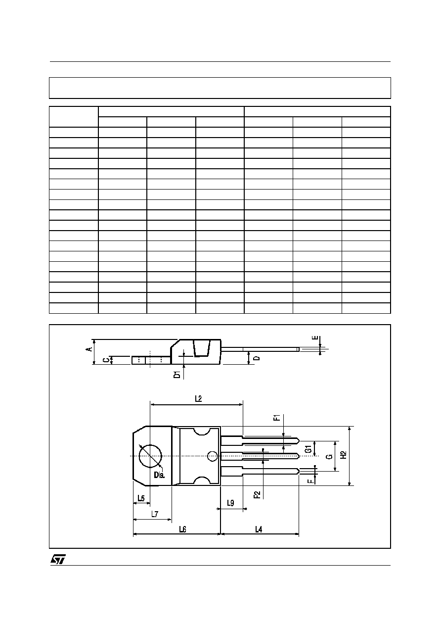
TO-220
�
1/6
THERMAL DATA
R
t hj-ca se
R
t hj- amb
Thermal Resistance Junction-Case
Max
Thermal Resistance Junction-Ambient
Max
1.56
62. 5
o
C/W
o
C/W
ELECTRICAL CHARACTERISTICS (T
case
= 25
o
C unless otherwise specified)
Symb ol
Parameter
Test Cond ition s
Mi n.
Typ .
Max.
Un it
I
CES
Collect or Cut-off
Current (V
BE
= 0)
V
CE
= 850 V
V
CE
= 850 V
T
j
= 125
o
C
100
500
�
A
�
A
I
EBO
Emitt er Cut-off Current
(I
C
= 0)
V
EB
= 9 V
100
�
A
BV
EBO
Emitt er-Base
Breakdown Volt age
(I
C
= 0)
I
E
= 10mA
10
18
V
V
CEO(sus )
Collect or-Emitter
Sustaining Voltage
(I
B
= 0)
I
C
= 10 mA
L = 25 mH
450
V
V
CE(sat )
Collect or-Emitter
Saturat ion Voltage
I
C
= 1 A
I
B
= 0.2 A
I
C
= 2 A
I
B
= 0.4 A
I
C
= 4 A
I
B
= 0.8 A
0.1
0.3
0.6
1.2
V
V
V
V
BE(s at)
Base-Emitt er
Saturat ion Voltage
I
C
= 1 A
I
B
= 0.2 A
I
C
= 4 A
I
B
= 0.8 A
1.0
1.3
V
V
h
FE
DC Current G ain
I
C
= 10 mA
V
CE
= 5 V
I
C
= 0. 5 A
V
CE
= 5 V
I
C
= 7 A
V
CE
= 10 V
10
4
60
10
V
CEW
Maximum Collect or
Emitt er Volt age
Without Snubber
I
C
= 8 A
R
BB
= 0
V
BB
= -2.5 V
L = 50
�
H
t
p
= 10
�
s
450
V
t
s
t
f
RESI STIVE LO AD
St orage Time
Fall T ime
I
C
= 2 A
V
CC
= 250 V
I
B(o n)
= I
B(of f)
= 0. 4 A
2
3
0.8
�
s
�
s
t
s
t
f
INDUCTIVE LOAD
St orage Time
Fall T ime
I
C
= 4 A
I
B(on )
= 0.8 A
V
BE(of f)
= -5 V
R
BB
= 0
V
CL
= 300 V
L = 1 mH
0.6
50
1.3
100
�
s
ns
V
f
Diode Forward Volt age
I
C
= 3 A
1.5
V
Pulsed: Pulse duration = 300
�
s, duty cycle 1.5 %
BUL49D
2/6