BUL59
HIGH VOLTAGE FAST-SWITCHING
NPN POWER TRANSISTOR
s
NPN TRANSISTOR
s
HIGH VOLTAGE CAPABILITY
s
MINIMUM LOT-TO-LOT SPREAD FOR
RELIABLE OPERATION
s
VERY HIGH SWITCHING SPEED
s
HIGH RUGGEDNESS
APPLICATIONS
s
ELECTRONIC TRANSFORMERS FOR
HALOGEN LAMPS
s
SWITCH MODE POWER SUPPLIES
DESCRIPTION
The BUL59 is manufactured using high voltage
Multi Epitaxial Mesa technology to enhance
switching speeds while maintaining wide RBSOA.
The BUL series is designed for use in lighting
applications and low cost switch-mode power
supplies.
Æ
INTERNAL SCHEMATIC DIAGRAM
June 2001
ABSOLUTE MAXIMUM RATINGS
Symbol
Parameter
Value
Unit
V
CES
Collector-Emitter Voltage (V
BE
= 0)
850
V
V
CEO
Collector-Emitter Voltage (I
B
= 0)
400
V
V
EBO
Emitter-Base Voltage (I
C
= 0)
9
V
I
C
Collector Current
8
A
I
CM
Collector Peak Current (t
p
<5 ms)
16
A
I
B
Base Current
4
A
I
BM
Base Peak Current (t
p
<5 ms)
8
A
P
tot
Total Dissipation at Tc = 25
o
C
90
W
T
stg
Storage Temperature
-65 to 150
o
C
T
j
Max. Operating Junction Temperature
150
o
C
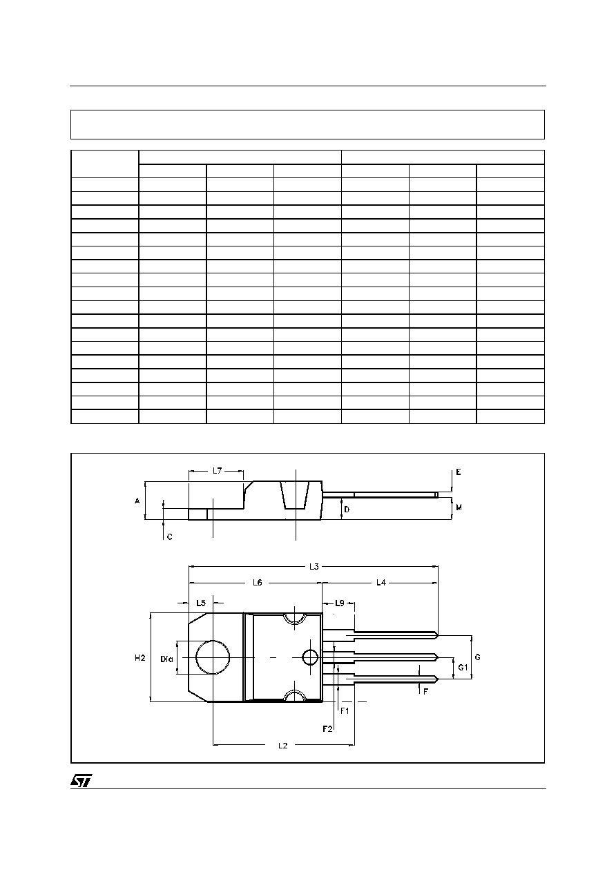
1
2
3
TO-220
1/6
THERMAL DATA
R
thj-case
R
thj-amb
Thermal Resistance Junction-Case Max
Thermal Resistance Junction-Ambient Max
1.39
62.5
o
C/W
o
C/W
ELECTRICAL CHARACTERISTICS (T
case
= 25
o
C unless otherwise specified)
Symbol
Parameter
Test Conditions
Min.
Typ.
Max.
Unit
I
CES
Collector Cut-off
Current (V
BE
= 0)
V
CE
= rated V
CES
V
CE
= rated V
CES
T
j
= 125
o
C
200
500
µ
A
µ
A
I
EBO
Emitter Cut-off Current
(I
C
= 0)
V
EB
= 9 V
100
µ
A
V
CEO(sus)
Collector-Emitter
Sustaining Voltage
(I
B
= 0)
I
C
= 10 mA L = 25 mH
400
V
V
CE(sat)
Collector-Emitter
Saturation Voltage
I
C
= 2 A I
B
= 0.4 A
I
C
= 5 A I
B
= 1 A
0.18
0.5
1.5
V
V
V
BE(sat)
Base-Emitter
Saturation Voltage
I
C
= 2 A I
B
= 0.4 A
I
C
= 5 A I
B
= 1 A
1.2
1.6
V
V
V
CEW
Maximum Collector
Emitter Voltage
Without Snubber
I
C
= 15 A R
BB
= 0
V
BB
= -2.5 V L = 50
µ
H
t
p
= 10
µ
s
450
V
h
FE
DC Current Gain
I
C
= 2 A V
CE
= 5 V
I
C
= 5 A V
CE
= 5 V
I
C
= 8 A V
CE
= 10 V
8
6
4
40
30
t
s
t
f
INDUCTIVE LOAD
Storage Time
Fall Time
I
C
= 2 A I
Bon
= 0.4 A
V
BE(o ff)
= -5 V R
BB
= 0
V
CC
= 250 V L = 200
µ
H
0.8
0.15
µ
s
µ
s
Pulsed: Pulse duration = 300
µ
s, duty cycle 1.5 %
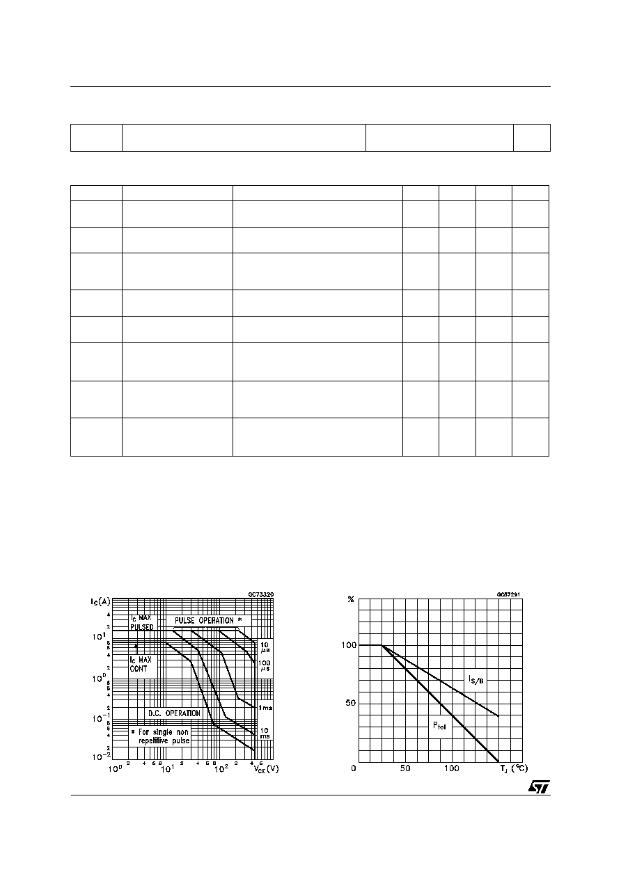
Safe Operating Areas
Derating Curve
BUL59
2/6
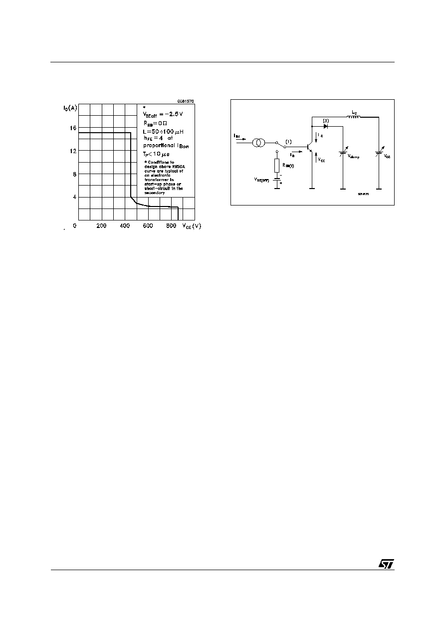
(1) Fast electronic switch
(2) Non-inductive Resistor
(3) Fast recovery rectifier
Reverse Biased SOA
RBSOA and Inductive Load Switching Test Circuit
BUL59
4/6