 | –≠–ª–µ–∫—Ç—Ä–æ–Ω–Ω—ã–π –∫–æ–º–ø–æ–Ω–µ–Ω—Ç: BUL804 | –°–∫–∞—á–∞—Ç—å:  PDF PDF  ZIP ZIP |

1/7
July 2005
n
NPN TRANSISTOR
n
HIGH VOLTAGE CAPABILITY
n
LOW SPREAD OF DYNAMIC PARAMETERS
n
MINIMUM LOT-TO-LOT SPREAD FOR
RELIABLE OPERATION
n
VERY HIGH SWITCHING SPEED
APPLICATIONS
n
DEDICATED FOR PFC SOLUTION IN
HALF-BRIDGE VOLTAGE FED TOPOLOGY
n
ELECTRONIC BALLAST FOR
FLUORESCENT LIGHTING
DESCRIPTION
The device is manufactured using high voltage
Multi Epitaxial Planar technology for high
switching speeds and medium voltage capability.
It uses a Cellular Emitter structure with planar
edge termination to enhance switching speeds
while maintaining the wide RBSOA.
The device is designed for use as PFC in high
frequency ballast half Bridge voltage fed topology.
Figure 1: Package
Figure 2: Internal Schematic Diagram
Table 1: Order Codes
1
2
3
TO-220
Part Number
Marking
Package
Packaging
BUL804
BUL804
TO-220
Tube
BUL804
HIGH VOLTAGE FAST-SWITCHING
NPN POWER TRANSISTOR
Rev. 1
BUL804
2/7
Table 2: Absolute Maximum Ratings
Table 3: Thermal Data
Table 4: Electrical Characteristics (T
case
= 25
o
C unless otherwise specified)
* Pulsed: Pulsed duration = 300 µs, duty cycle
1.5
%.
Symbol
Parameter
Value
Unit
V
CES
Collector-Emitter Voltage (V
BE
= 0)
800
V
V
CEO
Collector-Emitter Voltage (I
B
= 0)
450
V
V
EBO
Emitter-Base Voltage (I
C
= 0)
8
V
I
C
Collector Current
4
A
I
CM
Collector Peak Current (t
p
< 5ms)
8
A
I
B
Base Current
2
A
I
BM
Base Peak Current (t
p
< 5ms)
4
A
P
tot
Total Dissipation at T
C
= 25
o
C
70
W
T
stg
Storage Temperature
-65 to 150
∞C
T
J
Max. Operating Junction Temperature
150
∞C
R
thj-case
R
thj-amb
Thermal Resistance Junction-Case Max
Thermal Resistance Junction-Ambient Max
1.78
62.5
o
C/W
o
C/W
Symbol
Parameter
Test Conditions
Min.
Typ.
Max.
Unit
I
CES
Collector Cut-off Current
(V
BE
= -1.5 V)
V
CE
= 800 V
V
CE
= 800 V T
j
= 125
o
C
100
500
µA
µA
V
EBO
Emitter-Base Voltage
(I
C
= 0 )
I
E
= 10 mA
8
V
V
CEO(sus)
* Collector-Emitter
Sustaining Voltage
(I
B
= 0 )
I
C
= 100 mA L = 25 mH
450
V
I
CEO
Collector Cut-off Current
(I
B
= 0)
V
CE
= 450 V
250
µA
V
CE(sat)
*
Collector-Emitter
Saturation Voltage
I
C
= 1 A I
B
= 0.2 A
I
C
= 2.5 A I
B
= 0.5 A
0.8
1.2
V
V
V
BE(sat)
*
Base-Emitter Saturation
Voltage
I
C
= 1 A I
B
= 0.2 A
I
C
= 2.5 A I
B
= 0.5 A
1.2
1.3
V
V
h
FE
DC Current Gain
I
C
= 10 mA V
CE
= 5 V
I
C
= 2 A V
CE
= 5 V
10
10
20
t
s
t
f
RESISTIVE LOAD
Storage Time
Fall Time
V
CC
= 300 V I
C
= 2 A
I
B1
= 0.4 A I
B2
= -0.4 A
T
p
= 30 µs (see figure 11)
1.8
0.1
2.6
0.25
µs
µs
t
s
t
f
INDUCTIVE LOAD
Storage Time
Fall Time
I
C
= 2 A I
B1
= 0.4 A
V
BE(off)
= -5 V R
BB
= 0 W
V
clamp
= 360 V (see figure 10)
0.6
0.1
1
0.2
µs
µs
BUL804
3/7
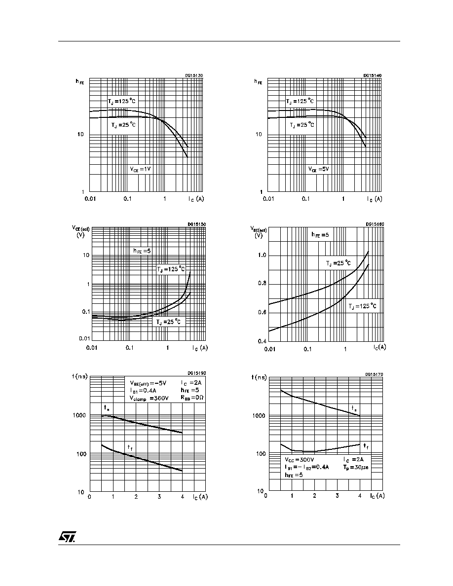
Figure 3: DC Current Gain
Figure 4: Collector-Emitter Saturation Voltage
Figure 5: Inductive Load Switching Time
Figure 6: DC Current Gain
Figure 7: Base-Emitter Saturation Voltage
Figure 8: Resistive Load Switching Time

BUL804
4/7
Figure 9: Reverse Biased Operating Area
Figure 10: Inductive Load Switching Test Circuit
Figure 11: Restistive Load Switching Test Circuit
1) Fast electronic switch
3) Fast recovery rectifier
2) Non-inductive Resistor
2) Non-inductive Resistor
1) Fast electronic switch
BUL804
5/7
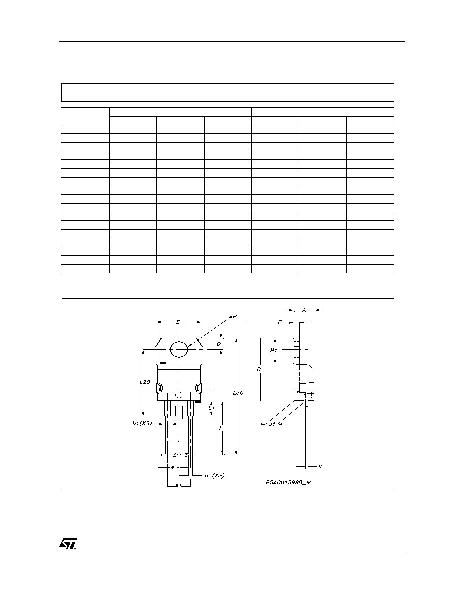
DIM.
mm.
inch
MIN.
TYP
MAX.
MIN.
TYP.
MAX.
A
4.40
4.60
0.173
0.181
b
0.61
0.88
0.024
0.034
b1
1.15
1.70
0.045
0.066
c
0.49
0.70
0.019
0.027
D
15.25
15.75
0.60
0.620
E
10
10.40
0.393
0.409
e
2.40
2.70
0.094
0.106
e1
4.95
5.15
0.194
0.202
F
1.23
1.32
0.048
0.052
H1
6.20
6.60
0.244
0.256
J1
2.40
2.72
0.094
0.107
L
13
14
0.511
0.551
L1
3.50
3.93
0.137
0.154
L20
16.40
0.645
L30
28.90
1.137
¯P
3.75
3.85
0.147
0.151
Q
2.65
2.95
0.104
0.116
TO-220 MECHANICAL DATA