BUL89
HIGH VOLTAGE FAST-SWITCHING
NPN POWER TRANSISTOR
s
HIGH VOLTAGE CAPABILITY
s
MINIMUM LOT-TO-LOT SPREAD FOR
RELIABLE OPERATION
s
LOW BASE-DRIVE REQUIREMENTS
s
VERY HIGH SWITCHING SPEED
s
FULLY CHARACTERIZED AT 125
o
C
APPLICATIONS
s
ELECTRONIC TRANSFORMER FOR
HALOGEN LAMPS
s
SWITCH MODE POWER SUPPLIES
DESCRIPTION
The BUL89 is manufactured using high voltage
Multiepitaxial Mesa technology for cost-effective
high performance. It uses a Hollow Emitter
structure to enhance switching speeds.
The BUL series is designed for use in lighting
applications and low cost switch-mode power
supplies.
Æ
INTERNAL SCHEMATIC DIAGRAM
January 2000
ABSOLUTE MAXIMUM RATINGS
Symbol
Parameter
Val ue
Uni t
V
CES
Collector-Emit ter Voltage (V
BE
= 0)
850
V
V
CEO
Collector-Emit ter Voltage (I
B
= 0)
400
V
V
EBO
Emitt er-Base Voltage (I
C
= 0)
9
V
I
C
Collector Current
12
A
I
CM
Collector Peak Current (t
p
< 5 ms)
25
A
I
B
Base Current
6
A
I
BM
Base Peak Current (t
p
< 5 ms)
12
A
P
t ot
Total Dissipation at T
c
= 25
o
C
110
W
T
stg
St orage Temperature
-65 to 150
o
C
T
j
Max. Operating Junction T emperature
150
o
C
1
2
3
TO-220
1/6

THERMAL DATA
R
t hj-ca se
Thermal Resist ance Junction-Case
Max
1.14
o
C/W
ELECTRICAL CHARACTERISTICS (T
case
= 25
o
C unless otherwise specified)
Symb ol
Parameter
Test Cond ition s
Mi n.
Typ .
Max.
Un it
I
CES
Collector Cut -of f
Current (V
BE
= 0)
V
CE
= 850 V
V
CE
= 850 V
T
j
= 125
o
C
100
500
µ
A
µ
A
I
CEO
Collector Cut -of f
Current (I
B
= 0)
V
CE
= 400 V
100
µ
A
V
CEO(sus )
Collector-Emit ter
Sustaining Voltage
(I
B
= 0)
I
C
= 10 mA
L = 25 mH
400
V
V
EBO
Emitt er-Base Volt age
(I
C
= 0)
I
E
= 10 mA
9
V
V
CE(sat )
Collector-Emit ter
Saturat ion Voltage
I
C
= 5 A
I
B
= 1 A
I
C
= 8 A
I
B
= 1.6 A
I
C
= 12 A
I
B
= 2. 4 A
1
1.5
5
V
V
V
V
BE(s at)
Base-Emitt er
Saturat ion Voltage
I
C
= 5 A
I
B
= 1 A
I
C
= 8 A
I
B
= 1.6 A
1.3
1.6
V
V
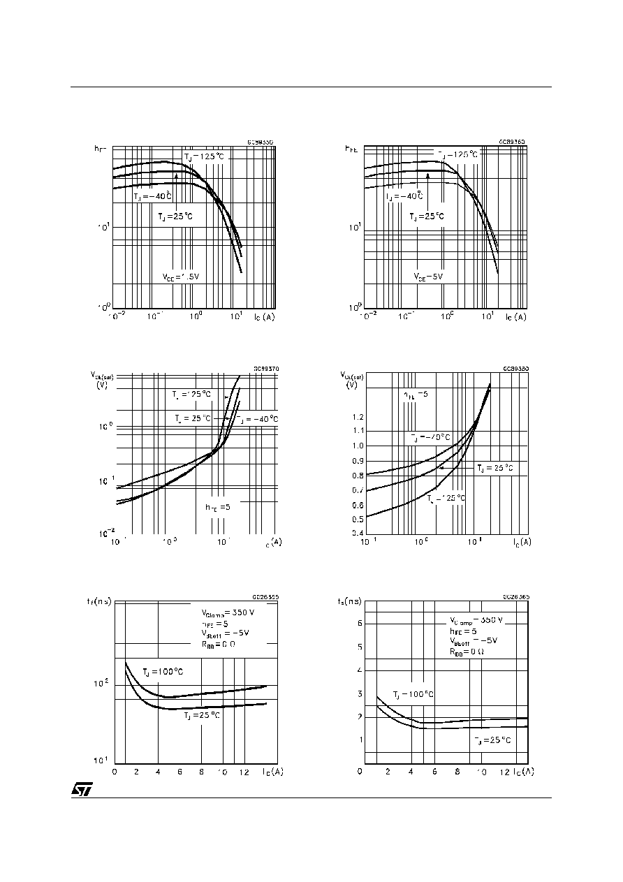
h
FE
DC Current G ain
I
C
= 5 A
V
CE
= 5 V
I
C
= 10 mA
V
CE
= 5 V
10
10
40
t
s
t
f
INDUCTIVE LOAD
St orage Time
Fall Time
I
C
= 8 A
I
B1
= 1.6 A
V
BE(of f)
= -5 V
R
BB
= 0
V
CL
= 350 V
L = 200
µ
H
1.5
55
2.3
110
µ
s
ns
t
s
t
f
INDUCTIVE LOAD
St orage Time
Fall Time
I
C
= 8 A
I
B1
= 1.6 A
V
BE(of f)
= -5 V
R
BB
= 0
V
CL
= 350 V
L = 200
µ
H
T
j
= 100
o
C
1.9
80
µ
s
ns
Pulsed: Pulse duration = 300
µ
s, duty cycle 1.5 %
Safe Operating Area
Derating Curve
BUL89
2/6

Reverse Biased SOA
RBSOA and Inductive Load Switching Test Circuit
(1) Fast electronic switch
(2) Non-inductive Resistor
(3) Fast recovery rectifier
BUL89
4/6