BULD1101ET4
HIGH VOLTAGE FAST-SWITCHING
NPN POWER TRANSISTOR
PRELIMINARY DATA
s
HIGH VOLTAGE CAPABILITY
s
LOW SPREAD OF DYNAMIC PARAMETERS
s
MINIMUM LOT-TO-LOT SPREAD FOR
RELIABLE OPERATION
s
VERY HIGH SWITCHING SPEED
s
LARGE RBSOA
s
SURFACE-MOUNTING DPAK (TO-252)
POWER PACKAGE IN TAPE & REEL
(SUFFIX "T4")
APPLICATIONS
s
ELECTRONIC BALLASTS FOR
FLUORESCENT LIGHTING
DESCRIPTION
The device is manufactured using High Voltage
Multi Epitaxial Planar technology for high
switching speeds and high voltage capability. It
uses a Cellular Emitter structure with planar edge
termination to enhance switching speeds while
maintaining a wide RBSOA.
INTERNAL SCHEMATIC DIAGRAM
April 2003
1
3
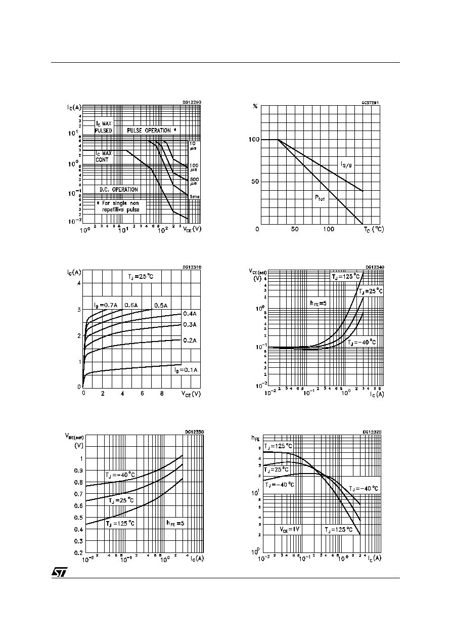
ABSOLUTE MAXIMUM RATINGS
Symbol
Parameter
Value
Unit
V
CES
Collector-Emitter Voltage (V
BE
= 0)
1100
V
V
CEO
Collector-Emitter Voltage (I
B
= 0)
450
V
V
EBO
Emitter-Base Voltage (I
C
= 0)
12
V
I
C
Collector Current
3
A
I
CM
Collector Peak Current (t
p
<5 ms)
6
A
I
B
Base Current
1.5
A
I
BM
Base Peak Current (t
p
<5 ms)
3
A
P
tot
Total Dissipation at Tc = 25
o
C
35
W
T
stg
Storage Temperature
-65 to 150
o
C
T
j
Max. Operating Junction Temperature
150
o
C
DPAK
TO-252
(Suffix "T4")
Æ
Ordering Code
Marking
Shipment
BULD1101ET4
BULD1101E
Tape & Reel
1/7

THERMAL DATA
R
thj-case
R
thj-amb
Thermal Resistance Junction-Case Max
Thermal Resistance Junction-ambient Max
3.57
100
o
C/W
o
C/W
ELECTRICAL CHARACTERISTICS (T
case
= 25
o
C unless otherwise specified)
Symbol
Parameter
Test Conditions
Min.
Typ.
Max.
Unit
I
CES
Collector Cut-off
Current (V
BE
= 0)
V
CE
= 1100 V
100
µ
A
V
(BR)EBO
Emitter-BaseBreakdown
Voltage (I
C
= 0)
I
E
= 1 mA
12
24
V
V
CEO(sus)
Collector-Emitter
Sustaining Voltage
(I
B
= 0)
I
C
= 100 mA
450
V
V
CE(sat)
Collector-Emitter
Saturation Voltage
I
C
= 1 A I
B
= 200 mA
I
C
= 1 A I
B
= 200 mA T
j
= 125
o
C
0.25
0.6
1
1.5
V
V
V
BE(sat)
Base-Emitter
Saturation Voltage
I
C
= 1 A I
B
= 200 mA
1.5
V
h
FE
DC Current Gain
I
C
= 250 mA V
CE
= 5 V
I
C
= 250 mA V
CE
= 5 V T
j
= 125
o
C
I
C
= 2 A V
CE
= 5 V
I
C
= 2 A V
CE
= 5 V T
j
= 125
o
C
20
23
6
4
38
44
10
7
80
85
18
16
t
s
t
f
RESISTIVE LOAD
Storage Time
Fall Time
I
C
= 2.5 A V
CC
= 125 V
V
BB(o ff)
= -5 V t
P
= 300
µ
s
I
B1
= -I
B2
= 0.5 A
(see figure 1)
400
2
700
µ
s
ns
E
ar
Repetitive Avalanche
Energy
L = 2 mH C = 1.8 nF
I
BR
2.5A (see figure 2)
6
mJ
Pulsed: Pulse duration = 300
µ
s, duty cycle 1.5 %
BULD1101ET4
2/7
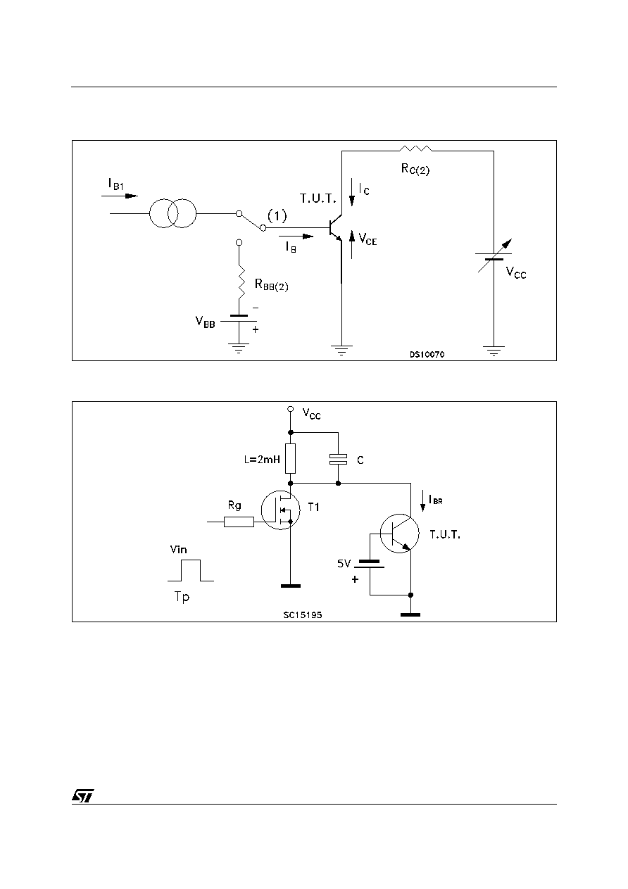
Figure 2: Energy Rating Test Circuit
Figure 1: Resistive Load Switching Test Circuit
1) Fast electronic switch
2) Non-inductive Resistor
3) Fast recovery rectifier
BULD1101ET4
5/7