 | –≠–ª–µ–∫—Ç—Ä–æ–Ω–Ω—ã–π –∫–æ–º–ø–æ–Ω–µ–Ω—Ç: BUTW92 | –°–∫–∞—á–∞—Ç—å:  PDF PDF  ZIP ZIP |
BUTW92
HIGH CURRENT NPN SILICON TRANSISTOR
s
SGS-THOMSON PREFERRED SALESTYPE
s
NPN TRANSISTOR
APPLICATIONS:
s
MOTOR CONTROL
s
HIGH FREQUENCY AND EFFICIENCY
CONVERTERS
DESCRIPTION
High current, high speed transistor suited for
power conversion applications, high efficency
converters and motor controls.
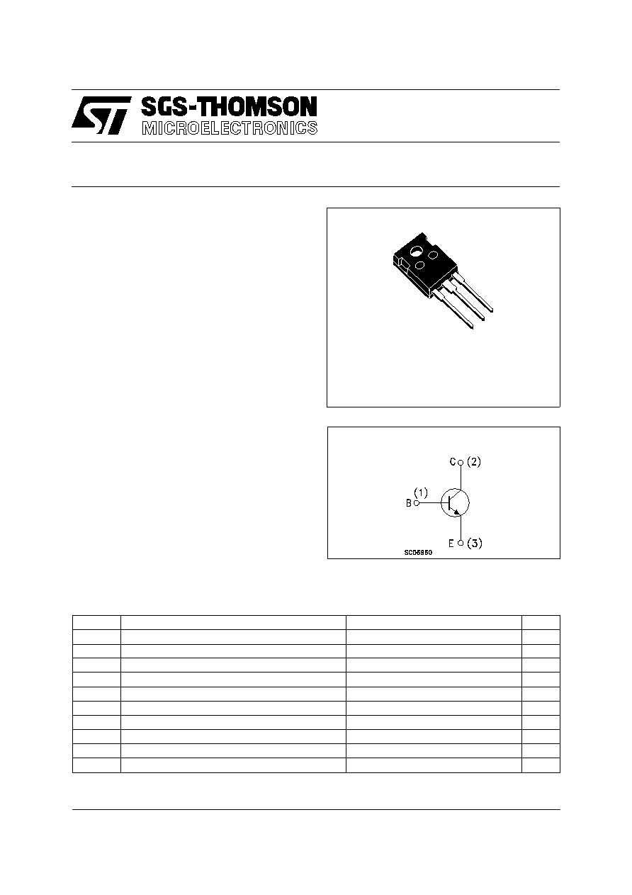
INTERNAL SCHEMATIC DIAGRAM
July 1997
ABSOLUTE MAXIMUM RATINGS
Symbol
Parameter
Value
Unit
V
CES
Collector-Emitter Voltage (V
BE
= 0)
500
V
V
CEO
Collector-Emitter Voltage (I
B
= 0)
250
V
V
EBO
Emitter-Base Voltage (I
C
= 0)
7
V
I
E
Emitter-Current
60
A
I
EM
Emitter Peak Current (t
p
< 5ms)
70
A
I
B
Base Current
15
A
I
BM
Base Peak Current (t
p
< 5ms)
18
A
P
tot
Total Dissipation at T
c
25
o
C
180
W
T
stg
Storage Temperature
-65 to 150
o
C
T
j
Max. Operating Junction Temperature
150
o
C
For PNP type voltage and current values are negative.
1
2
3
TO-247
1/4

THERMAL DATA
R
thj-case
Thermal Resistance Junction-case MAX
0.7
o
C/W
ELECTRICAL CHARACTERISTICS (T
case
= 25
o
C unless otherwise specified)
Symbol
Parameter
Test Conditions
Min.
Typ.
Max.
Unit
I
CES
Collector Cut-off
Current (V
BE
= -1.5V)
V
CE
= 450 V
VCE
= 450 V T
C
= 100
o
C
50
1
µ
A
mA
I
EBO
Emitter Cut-off Current
(I
C
= 0)
V
EB
= 5 V
50
µ
A
V
CES
Collector-Emitter
Breakdown Voltage
(V
EB
=0)
IC = 5 mA
500
V
V
EBO
Emitter-Base
Breakdown Voltage
(I
C
= 0)
I
E
= 50 mA
7
V
V
CEO(sus)
Collector-Emitter
Sustaining Voltage
(I
B
=0)
I
C
= 200 mA
250
V
V
CE(sat)
Collector-Emitter
Saturation Voltage
I
C
= 60 A I
B
= 15 A
I
C
= 60 A I
B
= 15 A T
C
= 100
o
C
0.8
1.1
1
1.5
V
V
V
BE(sat)
Base-Emitter
Saturation Voltage
I
C
= 60 A I
B
= 15 A
I
C
= 60 A I
B
= 15 A T
C
= 100
o
C
1.9
2
V
V
h
FE
DC Current Gain
I
C
= 60 A V
CE
= 3 V
I
C
= 60 A V
CE
= 3 V T
C
= 100
o
C
I
C
= 5 A V
CE
= 3 V
9
6
65
t
s
t
f
RESISTIVE LOAD
Storage Time
Fall Time
I
C
= 50 A V
CC
= 250 V
I
B1
= -I
B2
= 10 A
1.2
250
1.4
300
µ
s
ns
Pulsed: Pulse duration = 300
µ
s, duty cycle 1.5 %
BUTW92
2/4
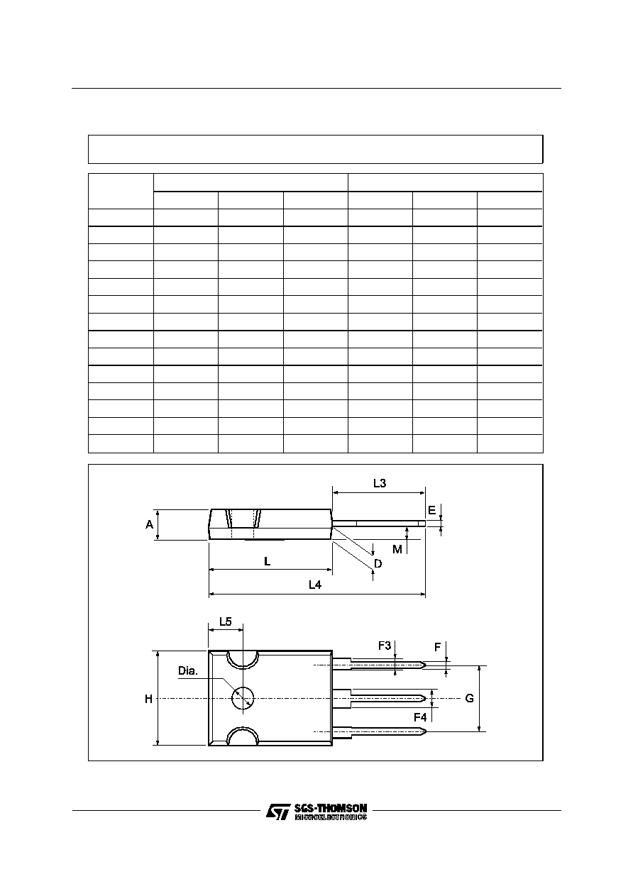
DIM.
mm
inch
MIN.
TYP.
MAX.
MIN.
TYP.
MAX.
A
4.7
5.3
0.185
0.209
D
2.2
2.6
0.087
0.102
E
0.4
0.8
0.016
0.031
F
1
1.4
0.039
0.055
F3
2
2.4
0.079
0.094
F4
3
3.4
0.118
0.134
G
10.9
0.429
H
15.3
15.9
0.602
0.626
L
19.7
20.3
0.776
0.779
L3
14.2
14.8
0.559
0.413
0.582
L4
34.6
1.362
L5
5.5
0.217
M
2
3
0.079
0.118
Dia
3.55
3.65
0.140
0.144
P025P
TO-247 MECHANICAL DATA
BUTW92
3/4

Information furnished is believed to be accurate and reliable. However, SGS-THOMSON Microelectronics assumes no responsability for the
consequences of use of such information nor for any infringement of patents or other rights of third parties which may results from its use. No
license is granted by implication or otherwise under any patent or patent rights of SGS-THOMSON Microelectronics. Specifications mentioned
in this publication are subject to change without notice. This publication supersedes and replaces all information previously supplied.
SGS-THOMSON Microelectronics products are not authorized for use as critical components in life support devices or systems without express
written approval of SGS-THOMSON Microelectonics.
© 1997 SGS-THOMSON Microelectronics - Printed in Italy - All Rights Reserved
SGS-THOMSON Microelectronics GROUP OF COMPANIES
Australia - Brazil - Canada - China - France - Germany - Italy - Japan - Korea - Malaysia - Malta - Morocco - The Netherlands -
Singapore - Spain - Sweden - Switzerland - Taiwan - Thailand - United Kingdom - U.S.A
. . .
BUTW92
4/4