1/5
BYW100-200
October 2001 - Ed: 4B
HIGH EFFICIENCY FAST RECOVERY RECTIFIER DIODE
Æ
Low voltage drop and rectifier suited for switching
mode base drive and transistor circuits.
DESCRIPTION
s
Very low conduction losses
s
Negligible switching losses
s
Low forward and reverse recovery times
s
The specifications and curves enable the
determination of trr and I
RM
at 100∞C under
users conditions.
FEATURES AND BENEFITS
Symbol
Parameter
Value
Unit
V
RRM
Repetitive peak reverse voltage
200
V
I
FRM
Repetitive peak forward current *
tp = 5µs F = 1KHz
80
A
I
F(AV)
Average forward current*
Ta = 95∞C
= 0.5
1.5
A
I
FSM
Surge non repetitive forward current
tp=10 ms Sinusoidal
50
A
T
stg
Storage temperature range
-65 +150
∞C
Tj
Maximum operating junction temperature
+ 150
∞C
T
L
Maximum lead temperature for soldering during 10s at 4mm from
case
230
∞C
* On infinitive heatsink with 10mm lead length
ABSOLUTE RATINGS (limiting values)
I
F(AV)
1.5 A
V
RRM
200 V
Tj (max)
150 ∞C
V
F
(max)
0.85 V
MAIN PRODUCT CHARACTERISTICS
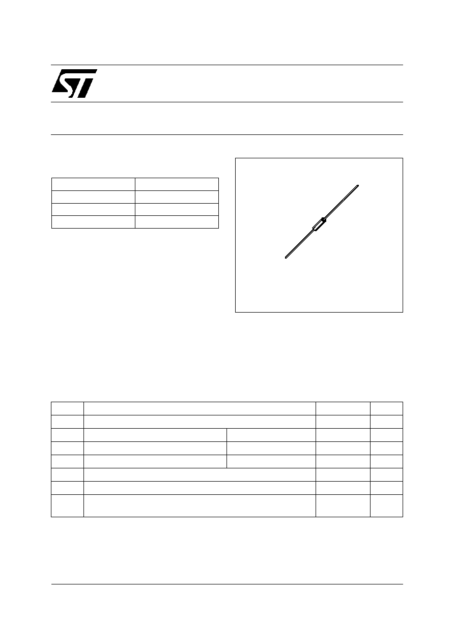
DO-15
BYW100-200
BYW100-200
2/5
Symbol
Parameter
Tests conditions
Min.
Typ.
Max.
Unit
I
R
*
Reverse leakage current
Tj = 25∞C
V
R
= V
RRM
10
µ
A
Tj = 100∞C
0.5
mA
V
F
**
Forward voltage drop
Tj = 25
∞
C
I
F
= 4.5A
1.2
V
Tj = 100∞C
I
F
= 1.5A
0.78
0.85
Pulse test : * tp = 5 ms,
< 2 %
** tp = 380
µ
s,
< 2 %
To evaluate the maximum conduction losses use the following equation :
P = 0.75 x I
F(AV)
+ 0.075 x I
F
2
(RMS)
STATIC ELECTRICAL CHARACTERISTICS
Symbol
Tests conditions
Min.
Typ.
Max.
Unit
trr
I
F
= 1A dI
F
/dt = - 50A/µs V
R
= 30V
Tj = 25∞C
35
ns
tfr
I
F
= 1.5A dI
F
/dt = - 50A/µs
Measured at 1.1 x V
F
max
Tj = 25∞C
30
ns
V
FP
I
F
= 1.5A dI
F
/dt = - 50A/µs
Tj = 25∞C
5
V
Qrr
I
F
= 1.5A dI
F
/dt = - 20A/µs V
R
30V
Tj = 25∞C
10
nC
RECOVERY CHARACTERISTICS
Symbol
Parameter
Value
Unit
R
th (j-a)
Junction to ambient*
45
∞
C/W
* On infinite heatsink with 10mm lead length.
THERMAL RESISTANCES

BYW100-200
3/5
5
10
15
20
25
0
10
20
30
40
50
60
70
80
90
100
110
Rth(∞C/W)
Rth(j-a)
Rth(j-l)
Lleads(mm)
Fig. 3: Thermal resistance versus lead length.
0.0 0.2 0.4 0.6 0.8 1.0 1.2 1.4 1.6 1.8 2.0 2.2 2.4 2.6
0.10
1.00
10.00
50.00
IFM(A)
Tj=25∞C
Tj=100∞C
Tj=100∞C
(Typical values)
VFM(V)
Fig. 5: Forward voltage drop versus forward
current (maximum values).
1E-2
1E-1
1E+0
1E+1
1E+2
5E+2
0.01
0.10
1.00
Zth(j-a)/Rth(j-a)
Single pulse
= 0.1
= 0.2
= 0.5
tp(s)
Fig. 4: Variation of thermal impedance junction to
ambient versus pulse duration (recommended pad
layout, epoxy FR4, e(Cu) = 35µm).
1
10
100
200
1
2
5
10
20
VR(V)
C(pF)
F=1MHz
Tj=25∞C
Fig. 6: Junction capacitance versus reverse
voltage applied (typical values).
0.0
0.2
0.4
0.6
0.8
1.0
1.2
1.4
1.6
1.8
0.0
0.2
0.4
0.6
0.8
1.0
1.2
1.4
1.6
PF(av)(W)
= 0.2
= 0.5
= 1
= 0.05
= 0.1
T
=tp/T
tp
IF(av) (A)
Fig. 1: Average forward power dissipation versus
average forward current.
0
25
50
75
100
125
150
0.0
0.2
0.4
0.6
0.8
1.0
1.2
1.4
1.6
1.8
IF(av)(A)
Rth(j-a)=100∞C/W
Rth(j-a)=Rth(j-l)
Tamb(∞C)
Fig. 2: Average forward current versus ambient
temperature (
=0.5).

BYW100-200
4/5
25
50
75
100
125
100
150
200
250
Tj(∞C)
%
IRM
Qrr
trr
Fig. 9: Dynamic parameters versus junction
temperature.
1
10
100
0
50
100
150
trr(ns)
IF=1.5A
VR=30V
90% confidence
Tj=100∞C
Tj=25∞C
dIF/dt(A/µs)
Fig. 7: Reverse recovery time versus dI
F
/dt.
1
10
100
0.0
0.5
1.0
1.5
2.0
2.5
IRM(A)
IF=1.5A
VR=30V
90% confidence
Tj=100∞C
Tj=25∞C
dIF/dt(A/µs)
Fig. 8: Peak reverse recovery current versus
dI
F
/dt.
BYW100-200
5/5
Ordering code
Marking
Package
Weight
Base qty
Delivery mode
BYW100-200
BYW100-200
DO-15
0.4 g
1000
Ammopack
BYW100-200RL
BYW100-200
DO-15
0.4 g
6000
Tape and reel
s
White band indicates cathode
s
Epoxy meets UL 94,V0
Information furnished is believed to be accurate and reliable. However, STMicroelectronics assumes no responsibility for the consequences of
use of such information nor for any infringement of patents or other rights of third parties which may result from its use. No license is granted by
implication or otherwise under any patent or patent rights of STMicroelectronics. Specifications mentioned in this publication are subject to
change without notice. This publication supersedes and replaces all information previously supplied.
STMicroelectronics products are not authorized for use as critical components in life support devices or systems without express written ap-
proval of STMicroelectronics.
The ST logo is a registered trademark of STMicroelectronics
© 2001 STMicroelectronics - Printed in Italy - All rights reserved.
STMicroelectronics GROUP OF COMPANIES
Australia - Brazil - Canada - China - Finland - France - Germany
Hong Kong - India - Israel - Italy - Japan - Malaysia -Malta - Morocco - Singapore
Spain - Sweden - Switzerland - United Kingdom - United States.
http://www.st.com
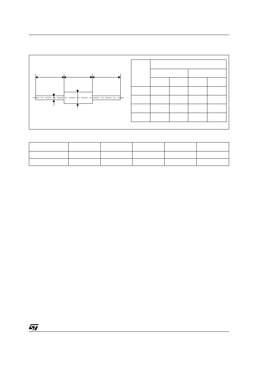
PACKAGE MECHANICAL DATA
DO-15
A
C
C
D
B
REF.
DIMENSIONS
Millimeters
Inches
Min.
Max.
Min.
Max.
A
6.05
6.75
0.238
0.266
B
2.95
3.53
0.116
0.139
C
26
31
1.024
1.220
D
0.71
0.88
0.028
0.035