 | –≠–ª–µ–∫—Ç—Ä–æ–Ω–Ω—ã–π –∫–æ–º–ø–æ–Ω–µ–Ω—Ç: CB35000 | –°–∫–∞—á–∞—Ç—å:  PDF PDF  ZIP ZIP |
CB35000 SERIES
HCMOS STANDARD CELLS
PRELIMINARY DATA
July 1995
1/16
Æ
FEATURES
s
0.5 micron triple layer metal HCMOS5S pro-
cess featuring retrograde well technology,
low resistance salicided active areas, polysi-
licide gates and thin metal oxide.
s
3.3 V optimized transistor with 5 V I/O inter-
face capability
s
2 - input NAND delay of 210 ps (typ) with
fanout = 2.
s
Broad I/O functionality including LVCMOS,
LVTTL, GTL, PECL, and LVDS.
s
High drive I/O; capability of sinking up to 48
mA with slew rate control, current spike sup-
pression and impedance matching.
s
Generators to support SPRAM, DPRAM,
ROM and MULT with BIST options.
s
Extensive embedded function library includ-
ing DSP and ST micros, popular third party
micros and Synopsys synthetic libraries.
Table 1
Module Generator Library
Cell
Description
SPRAM
256K bits max
16K word max 64 bit max
Zero static current
Tristate outputs
DPRAM
128K bits max
8K word max 64 bit max
Zero static current
Tristate outputs
ROM
2M bits max
32K word max 64 bit max
Diffusion programmable
Tristate outputs
MULT
Parallel asynchronous operation
2's complement product
6 to 64 bits for both inputs
Ripple Carry or Fast Carry Look Ahead
s
Fully independent power and ground config-
urations for inputs, core and outputs.
s
I/O ring capability up to 800 pads.
s
Output buffers capable of driving ISA, EISA,
PCI, MCA, and SCSI interface levels.
s
Active pull up and pull down devices.
s
Buskeeper I/O functions.
s
Oscillators for wide frequency spectrum.
s
Broad range of 300 SSI cells.
s
Low Power / Low Drive library subset.
s
Design For Test includes IEEE 1149.1 JTAG
Boundary Scan architecture built in.
s
Cadence and Mentor based design system
with interfaces from multiple workstations.
s
Broad ceramic and plastic package range.
s
Latchup trigger current > +/- 500 mA.
ESD protection > +/- 4000 volts.
CB35000 SERIES
2/16
Æ
GENERAL DISCRIPTION
The CB35000 standard cell series uses a high
performance, low voltage, triple level metal,
HCMOS5S 0.5 micron process to achieve sub-
nanosecond internal speeds while offering very
low power dissipation and high noise immunity.
With an average gate density of 5500 gates/mm
2
,
the CB35000 family allows the design of highly
complex devices. The potential available gate
count ranges above 1.5 Million equivalent gates.
Devices can operate over a Vdd voltage range of
2.7 to 3.6 volts.
The I/O count for this array family ranges to over
600 signals and 800 pins dependent upon the
package technology utilized. A Sea of I/O
approach has been followed to give a solution to
CONVENTIONAL VIA LAYOUT
STACKED VIA LAYOUT
SUBSTRATE
ISOLATION
GATE
CONTACT
METAL 1
METAL 2
METAL 3
1st VIA
2nd VIA
3rd DIELECTRIC
2nd DIELECTRIC
1st DIELECTRIC
AREA SAVINGS UP TO 20% FOR RANDOM LOGIC
SIMPLIFIED ROUTING AND DESIGN RULE CHECKING
CONTACT / VIA
PLUGS
Figure 1
Advantages of stacked contacts and vias
today's problems of drive levels and specialized
interface standards. The technology does not
utilize a set bond pad spacing but allows for pad
spacings from 80 microns upwards. The I/O is
fully compatible with that of the ISB35000
Structured Array family.
The I/O can be configured for circuits ranging
from low voltage CMOS and TTL to 350 mHz
plus low swing differential circuits. Standards like
GTL, SCSI-2, 3.3 Volt PCI, CTI, and a limited set
of 5.0 Volt interfaces are currently being
addressed. A specialized set of impedance
matched transmission line driver LVTTL type
circuits are also available with 25, 35, 45, and 55
Ohm output impedance. These buffers sacrifice
direct current capabilities for matching positive
and negative voltage and current waveforms.
3/16
CB35000 SERIES
Æ
LIBRARY OVERVIEW
The design of the CB35000 family has been
optimized to allow extremely high density, high
speed and low power designs. For these reasons
a wide range of cells with different ranges of
driving capability are available in the library.
The library cells have been optimized in term of
functional and electrical parameters in order to
have:
s
Good balancing
s
Maximum speed
s
Optimum Threshold voltage
s
Symmetric Vdd/Vss Noise margin
s
Minimum Power-Speed figure
Surrounding the core are configurational
specialized transistors forming a Sea of I/O giving
a high degree of flexibility to the system designer.
The geometrical aspect of the cells was
configured to allow extremely dense design, fully
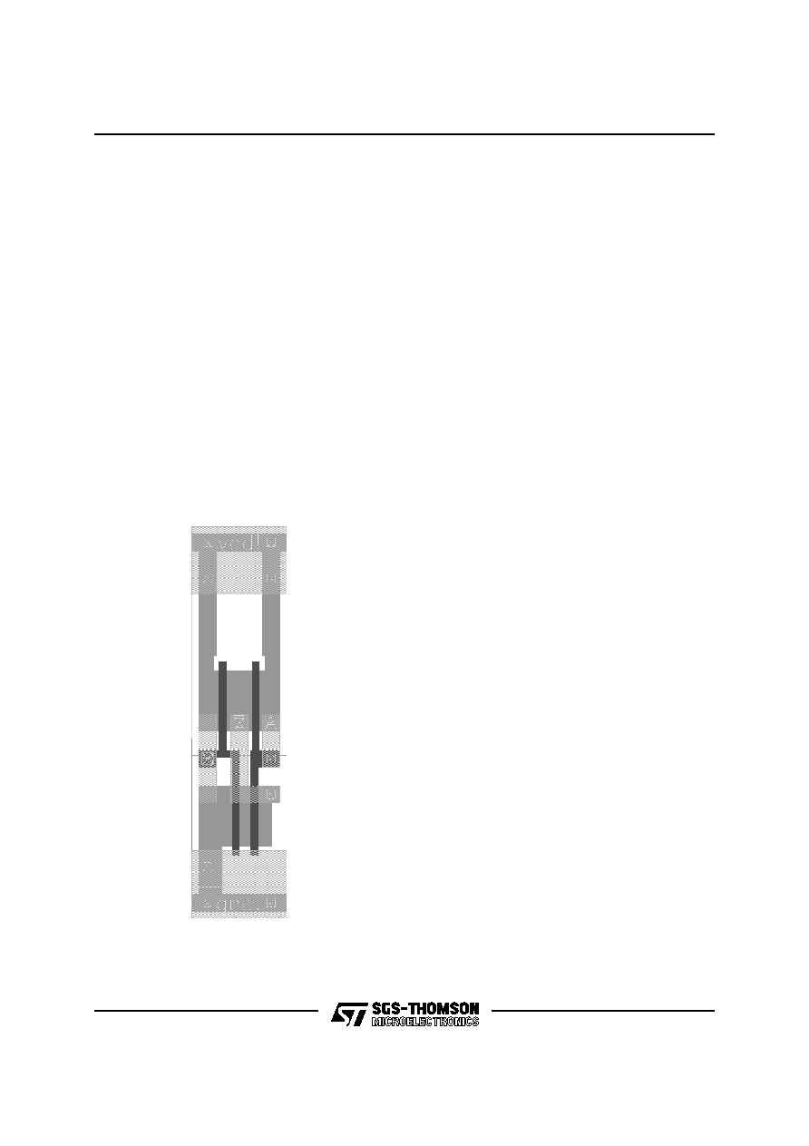
10 m
Figure 2. ND2 Core Cell
exploiting the features of the Place and Route
tool in terms of horizontal and vertical routing
grids. For Place and Route, three levels of metal
are utilized. Intracell and intercell wiring are
limited to first metal, with second and third metal
levels dedicated to interconnect wiring and power
distribution. Each cell gives the possibility to use
10 horizontal wiring channels using third metal.
With the horizontal grid unit being the same as
the Metal 2 minimum contacted pitch, the vertical
wiring can be done on every grid point, without
limitation.
TECHNOLOGY OVERVIEW
A major feature of the HCMOS5S process is
salicided active areas. This results in source
drain areas that are of one to two ohms
resistance as opposed to the hundreds or
thousands of ohms of source drain resistance in
previous technologies. This very low resistance is
one reason that very low transistor widths could
be utilized in the cell design since drive is not lost
due to source drain resistance. This use of low
width transistors results in lower capacitance
loading of the gates due to the smaller areas
utilized. Low resistance, low capacitance, and
small gates results in low power usage for
inverters as compared to previous technologies.
The reduction in power consumption allows the
usage of salicided active stripes to distribute
power internally to the simple cell, replacing, in
some cases, the usage of the first metal layer.
This saves silicon area by allowing greater
density, permeability and routability of the cells
resulting in greater overall circuit density.
The standard power distributions are Internal Vdd
and Vss, serving the internal cells and the
prebuffer sections of the I/O, External Vdd and
Vss serving the output transistors only, and
Receiver Vdd and Vss serving the first stages of
the receiver cells. Optional distributions for 5.0V
interface, GTL, CTL, and other standards can be
utilized as necessary.
CB35000 SERIES
4/16
Æ
LIBRARY
The following section details the elements which
make up the CB35000 Series library. The
elements are organized into three categories:
1. Macrocell library with Input, Output,
Bidirectional Buffers including JTAG
macrocells and Core cells.
2. Macrofunctions
3. Module generators.
I/O BUFFERS
CB35000 technology does not utilize a standard
type I/O cell but is a leader in the emerging Sea
of I/O approach to handling the chip interface
problem. This approach starts at the bond pad
area of the I/O where the pad size and pitch is not
determined until the customers choice of
packaging, signal interface standards and I/O
count is considered. Wire bond pad spacings for
80 micron centres are available where large
signal counts are most important.
Pad spacing can be increased incrementally. It is
expected that most designs will use 100 micron
spacings or above. It is also possible to use
different spacings for different width output
sections when needed within the same device.
Along with the variable bond pad spacing the I/O
output transistor section does not have a fixed
width. Previous technologies utilized a design
approach where the desired full function buffer
was designed for a maximum current taking one
pad location with the usual current in the range of
twenty four milliamps. The approach followed in
CB35000 is to have identical twenty five micron
wide output transistor slices stepped around the
die. Each slice contains one set of protection
diodes to the external power rails and eight P and
eight N transistors. The transistors are
specifically laid out and selectively non salicided
for ESD protection and latch up prevention.
These slices are paralleled to meet the current
needs of the user, for example, to construct a
24mA sink and 12mA source LVTTL buffer, a
number of slices would be used. The next group
of devices that makes up the I/O circuits is again
a 25u wide slice of specialized transistors that are
utilized to form the slew rate control sections of
the I/O. Each of these slices has circuits to
control the switching of up two sections of P and
N output transistors. These sections are of
course created from the output transistor slice
above the slew rate section and can be
connected as desired by the designer. Many
configurations of circuits can be created to supply
the desired results with slew rate slices paralleled
with multiple output sections. A further function of
the I/O circuits is current spike suppression
during switching of the I/O transistors. The logic
utilized causes the conducting transistors to turn
off before the opposing set of transistors turn on.
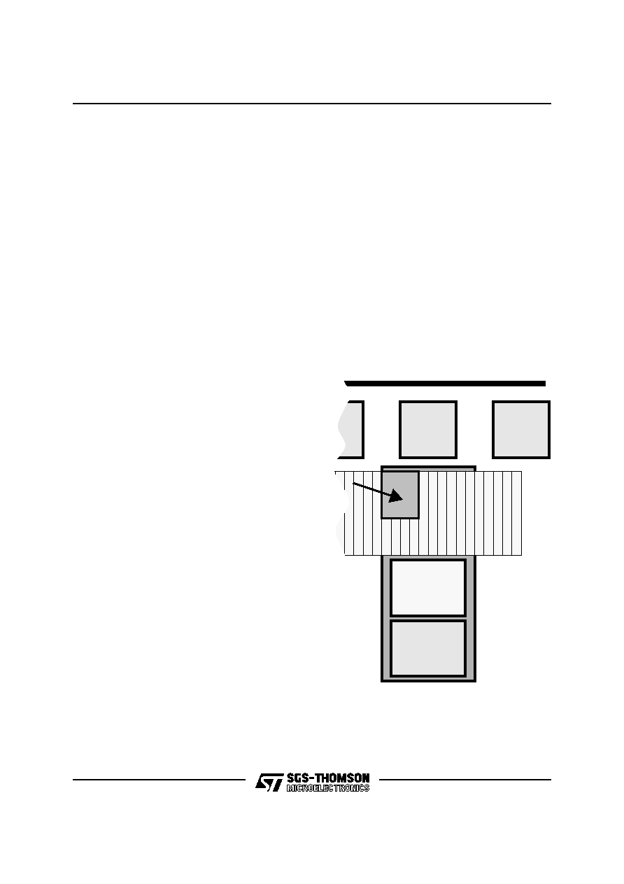
Figure 3
IO Buffer Technology
INPUT
CONTROL
SLEW RATE
TRISTATE
BUSKEEPER
LEVEL SHIFTER
PROGRAMMABLE
PITCH BOND PADS
DIE CORE
GUARDRING
EDGE OF DIE
SEGMENTED
OUTPUT
RIVER OF DRIVE
TRANSISTORS
4mA
Selected
5/16
CB35000 SERIES
Æ
Table 2
I/O Drive Capacity for LVCMOS and
LVTTL Slew Rate Buffers
Current Drive
(mA)
Maximum
Capacitance (pF)
2.0
50
4.0
100
8.0
200
12.0
300
16.0
400
24.0
800
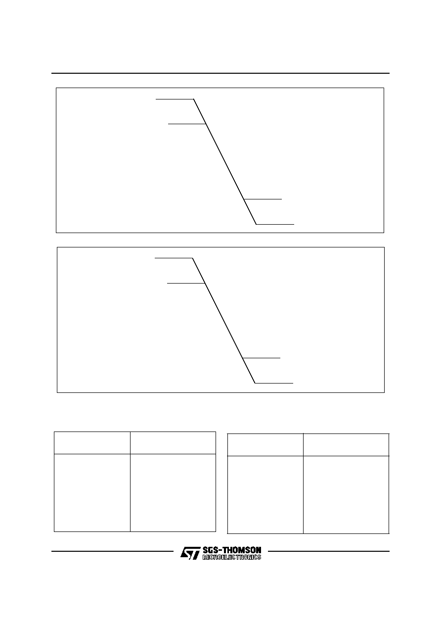
MPUL
LPUL
LPDL
MPDL
Vdd + 0.3 Volts
0.8 * Vdd
0.2 * Vdd
Vss - 0.3 Volts
Typical Current from all Vdd
supplies at LPUL or MPDL
25
µ
A per receiver
Trip Level = 0.5 * Vdd
Figure 4a
D.C. Specifications for
LVCMOS Input Receivers
MPUL
LPUL
LPDL
MPDL
Vdd + 0.3 Volts
Vss + 2.0 Volts
Vss + 0.8 Volts
Vss - 0.3 Volts
Typical Current from all Vdd
supplies at LPUL or MPDL
25
µ
A per receiver
Trip Level = 1.4 Volts
(nominal)
Figure 4b
D.C. Specifications for
LVTTL Input Receivers
Table 3
I/O Drive Capacity for LVCMOS and
LVTTL Non Slew Rate Buffers
Current Drive
(mA)
Maximum
Capacitance (pF)
2.0
50
4.0
100
8.0
200
12.0
300
16.0
400
24.0
800