1/10
CLT3-4BT6
August 2002 - Ed: 4A
CURRENT LIMITED OVER-VOLTAGE PROTECTED
QUAD DIGITAL TERMINATION
Æ
s
Reduced overall dissipation
s
Compact with high integration
s
Enables input to meet type 1 characteristic of IEC61131-2 standard
s
Compatible operation with 2 and 3 wires proximity sensor according EN60947-5-2 standard
s
Insensitive to the on state sensor impedance
s
Surface Mount Package for highly automated assembly
s
Enhanced functional reliability
BENEFITS
s
4 channels topology
s
Wide range input DC Voltage:
s
V
I
= - 0.3 to 30V with R
I
= 0
s
V
I
= - 30 to 35V with R
I
= 1.2k
s
Low side configuration with common ground
s
Current limiter:
s
I
GEN
= 3mA
s
Input current limiter activation voltage < 5V
s
Temperature compensated operation
s
Opto-coupler drive:
s
No coupler activation below 1.5 mA input current
s
Input protection (R
I
= 1.2K
):
s
IEC61000-4-2 electrostatic discharge ESD, Class 3
t
In contact, ±6kV; in air, ±8kV
t
Level B: temporary disruption; no change of opto-coupler state
s
IEC61000-4-5 voltage surge, Class 3
t
± 1000V with 42
serial resistor in differential mode
t
Level B: temporary disruption
s
IEC61000-4-4 transient burst immunity
t
± 4kV peak voltage; 5kHz repetitive rate
t
Level A: fully functional
s
Operating ambient temperature: - 25 to 85∞C
FEATURES
TSSOP20
s
Industrial Automation
s
Programmable Logic Controller
s
Communication field bus nodes
s
Peripheral Input / Output modules
s
Machine tool interface
APPLICATIONS
CLT3-4BT6
2/10
R
I
24V
SUPPLY
R
I
R
I
R
I
R
C
V
IN
V
I
V
CC
V
C
COM
COM
IN
1
ESD
12
IN
2
OUT
1
OUT
2
OUT
4
OUT
3
COM
34
ESD
34
COM
COM
IN
3
IN
4
COM
12
V
C
ESD
C
COM
COM
1
V
I
1
12
2
1
2
3
12
C
C
1
12
2
1
2
3
12
C
C
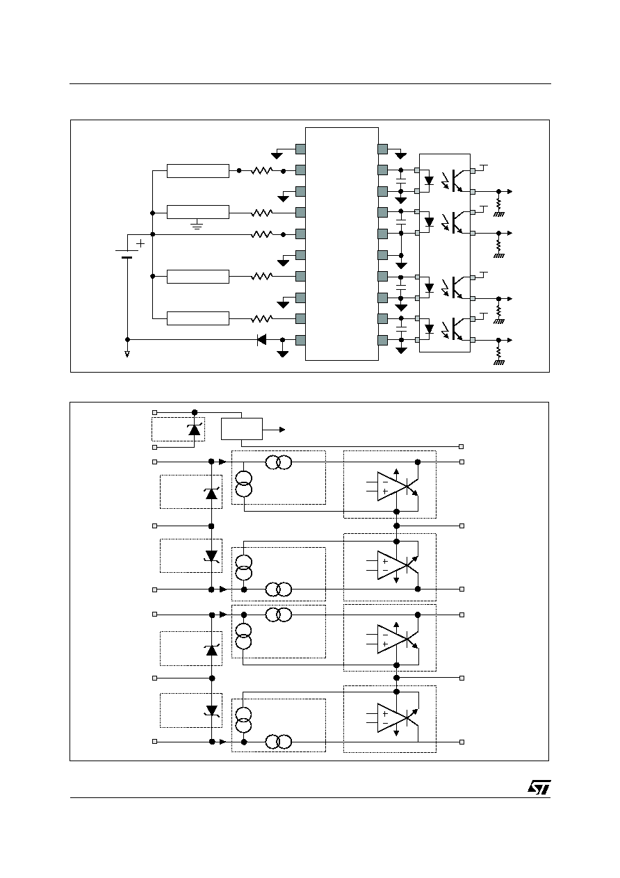
2 wires sensor
3 wires sensor
Contact switch
2 wires sensor
IEC61000-4 STANDARD ROBUST APPLICATION DIAGRAM
ESD
Volt Prot
Vc
COM
TO COMPARATORS
ESD
34
ESD
12
COM
12
OPTO COUPLER DRIVER
ESD
OVER
VOLTAGE
PROTECTION
IN
1
OUT
1
I
1
I
1
1.5mA
0.75xI
LIM
0.25xI
LIM
OPTO COUPLER DRIVER
OUT
2
ESD
C
COM
34
IN
4
CURRENT LIMITER I
LIM
BIASING
CIRCUIT
ESD
OVER
VOLTAGE
PROTECTION
0.25xI
LIM
0.75xI
LIM
1.5mA
I
2
CURRENT LIMITER I
LIM
I
2
IN
2
IN
3
ESD
OVER
VOLTAGE
PROTECTION
I
3
OPTO COUPLER DRIVER
0.75xI
LIM
0.25xI
LIM
CURRENT LIMITER I
LIM
OUT
3
I
3
1.5mA
0.25xI
LIM
0.75xI
LIM
ESD
OVER
VOLTAGE
PROTECTION
CURRENT LIMITER I
LIM
OPTO COUPLER DRIVER
1.5mA
I
4
OUT
4
I
4
INPUT TERMINATION BLOCK DIAGRAM
CLT3-4BT6
3/10
The CLTx-4 is a quadruple input digital termination device designed for 24 V DC automation applications. It
achieves the front-end circuitry of a digital input module (I/O) in industrial automation, and drives an
isolating opto-coupler.
Available in a four channels configuration, it offers a high-density termination by minimizing the external
components count. It is housed in a TSSOP20 surface mount package to reduce the printed board size.
Made of an input voltage protection, a serial current limiting circuit and an opto-coupler driver, each
channel circuit terminates the connection between the logic input and the associated high side sensor or
switch.
The CLT3-4 is a 3 mA quad channel device compatible the type 1 characteristics of the IEC61131-2
standard.
Each input voltage clamping block protects the module input against electromagnetic interferences such
as those described in the IEC61131-2 standard and IEC61000-4-2 (ESD), 4-4 (transient burst), 4-5
(voltage surge) standards. The supply input is also designed with such a protection structure.
The current limiting circuit connected between the input and the output pins is compensated all over the
temperature range. Thanks to its low tolerance, the current limitation allows reducing drastically the
dissipation of the input compared to a resistive input: the overall module requires less cooling capability
and becomes smaller.
The output block of each termination channel controls the operation of an opto-coupler that is enabled by a
Light Emitting Diode.
When the input current is less than 1.5 mA, this output circuit derivates the input current to maintain the
opto-coupler off.
The original structure of the CLT limiter allows its activation threshold to be low and insensitive to the
output voltage up to a maximum value of 2.0 V.
When the CLT input voltage V
IN
is higher than 5 V, or the module input voltage Vi higher than 11 V with the
use of a reverse diode and a serial resistor R
I
= 1.2 k
, the output current that is a share of the input current
(3/4) is higher than 1.5 mA. The whole termination channel including the opto-coupler is on.
FUNCTIONAL DESCRIPTION
Symbol
Pin
Parameter name & conditions
Value
Unit
V
CC
V
C
Supply steady state voltage, R
C
= 0k
- 0.3 to 30
V
Supply steady state voltage, R
C
= 4.7k
- 0.3 to 35
V
V
I
(1)
IN
Input steady state voltage, R
I
= 0k
- 0.3 to 30
V
Input steady state voltage, R
I
= 1.2k
- 0.3 to 32
V
Input repetitive pulse voltage, R
I
= 1.2k
- 0.3 to 35
V
Input repetitive pulse voltage,
R
I
= 1.2k
, R
C
= 4.7k
(2)
- 30 to 30
V
I
IN
IN
Input maximum forward current,
R
I
= 1.2k
, R
C
= 4.7k
5
mA
Input maximum reverse current,
R
I
= 1.2k
, R
C
= 4.7k
(2)
20
mA
V
OM
OUT
Maximum output steady state voltage
2.5
V
I
OM
OUT
Output current
- 4 to 4
mA
T
AMB
AII
Operating ambient temperature
- 25 to 85
∞C
T
J
Operating and storage junction temperature
- 25 to 150
∞C
Note 1: VI = VIN + RI x IIN; VIN = voltage at the input pin itself
Note 2: according to test diagram on figure 8, this case covers especially the reverse polarity operation of one input.
ABSOLUTE RATINGS (limiting values)
CLT3-4BT6
4/10
Symbol
Pin
Name
Conditions
Min.
Typ.
Max.
Unit
Current limitation
I
LIM
IN
Input limiting current
V
OUT
= 0.9 to 2.0V
V
IN
= 5 to 27V
T
AMB
= - 25 to 85∞C
2.1
3
3.7
mA
V
LOW
IN
Maximum off state volt-
age
I
IN
= 100µA
1.5
V
V
TH
IN
Activation threshold
I
IN
= 2.1 mA
3.4
5
V
Input & Supply Protection
V
CL
IN
Clamping voltage
I
IN
= 7mA; t
P
= 1 ms
31
38
-
V
Opto-coupler driver operation
I
OFF
OUT
Off state output current
V
I
= 5V, (5)
-
10
40
µA
I
IN
= 1.5mA, (6)
-
10
40
µA
V
OFF
OUT
Off state output voltage
I
IN
= 1.5 mA
0.15
0.5
V
I
ON
OUT
On state output current
V
IN
= 5V
1.5
2
-
mA
Supply & biasing circuit
V
C
V
C
Supply voltage
T
AMB
= - 25 to 85∞C
10
V
I
C
V
C
Supply current
V
IN
= V
C
= 30V
550
800
µA
Note 5: According to application diagram on page 2 with use of a RI = 1.2k
resistor, an opto-coupler (RLED (0V) = 15k
, VF = 1.2V) and a re-
verse diode from COM to GND (VF = 0.7V)
Note 6: same as note 5 but RI = 0
.
ELECTRICAL CHARACTERISTICS
(T
J
= 25∞C, V
CC
= 24V and COM pin voltage referred unless otherwise specified)
Symbol
Parameter
Value
Unit
R
th (j-a)
TSSOP20 thermal resistance junction to ambient
Board copper surface = 2cm≤, copper thickness = 35µm
90
∞
C/W
THERMAL RESISTANCE
Symbol
Node
Parameter name & conditions
Value
Unit
V
PP
IN
ESD protection, IEC61000-4-2, per input, in air
± 8
kV
ESD protection, IEC61000-4-2, per input, in contact
± 6
kV
ESD protection, IEC61000-4-2, per input, in air, R
I
= 0
± 3
kV
ESD protection, IEC61000-4-2, per input, in contact, R
I
= 0
± 3
kV
V
PPB
V
I
Total Peak Pulse Voltage Burst, IEC61000-4-4
C
IN
= 100pF, C
OUT
= 22nF, F = 5kHz (3)
± 4
kV
V
PP
VI
Peak Pulse Voltage Surge, IEC61000-4-5, R = 42
, (4)
± 1
kV
V
PP
V
CC
Peak Pulse Voltage Surge, IEC61000-4-5, R = 2
(4)
± 1
kV
Note 3: test conditions of IEC standard applied to the application diagram page 2.
Note 4: see test circuit figure 6 or 7.
ELECTROMAGNETIC COMPATIBILITY RATINGS
R
I
= 1.2k
, R
C
= 4.7k
, reverse diode connected as shown on figure 6 (unless otherwise specified)
CLT3-4BT6
5/10
Symbol
Pin
Name
Conditions
Min.
Typ.
Max.
Unit
F
MAX
IN-OUT
Input to output running frequency
200
Hz
t
PLH
IN-OUT
Input activation propagation time
C
OUT
= 22nF
6
µs
t
PHL
IN-OUT
Input de-activation propagation
time
C
OUT
= 22nF
10
µs
SWITCHING ELECTRICAL CHARACTERISTICS
(T
J
= 25∞C, V
CC
= 24V and COM pin voltage referred unless otherwise specified)
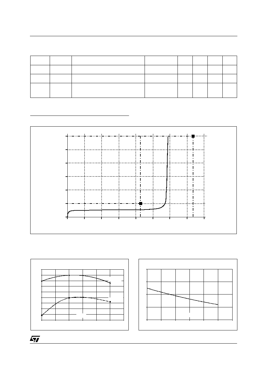
INPUT CHARACTERISTICS OF CLT3-4
30
25
20
15
10
5
0
30
5
2.1
3.7
0
0.5
1
1.5
2
2.5
3
3.5
4
V (V)
IN
I (mA)
IN
Fig. 1: Typical input characteristics of each CLT3-4 channel
IIim / IIim (25∞C)
84%
86%
88%
90%
92%
94%
96%
98%
100%
102%
-25
0
25
50
75
100
125
V
IN
= 27 V
V
IN
= 5 V
Tj (∞C)
Fig. 2: Typical current limiter variation versus junc-
tion temperature 0.9V < V
OUT
< 2V
3.2
3.3
3.4
3.5
3.6
-25
0
25
50
75
100
125
Tj (∞C)
VTH (V)
Fig. 3: Typical limiter threshold voltage variation
versus junction temperature for I
IN
= 2.1mA