 | –≠–ª–µ–∫—Ç—Ä–æ–Ω–Ω—ã–π –∫–æ–º–ø–æ–Ω–µ–Ω—Ç: D16NF06 | –°–∫–∞—á–∞—Ç—å:  PDF PDF  ZIP ZIP |
Rev 1
January 2006
1/11
11
STD16NF06
N-Channel 60V - 0.060
- 16A - DPAK
STripFETTM II Power MOSFET
General features
Typical R
DS(on)
= 0.060
Exceptional dv/dt Capability
100% Avalanche Tested
Application Oriented Characterization
Description
This Power MOSFET is the latest development of
STMicroelectronis unique "Single Feature SizeTM"
strip-based process. The resulting transistor
shows extremely high packing density for low
on-resistance, rugged avalanche characteristics
and less critical alignment steps therefore a
remarkable manufacturing reproducibility
Applications
Audio Amplifiers
Power Tools
Automotive Environment
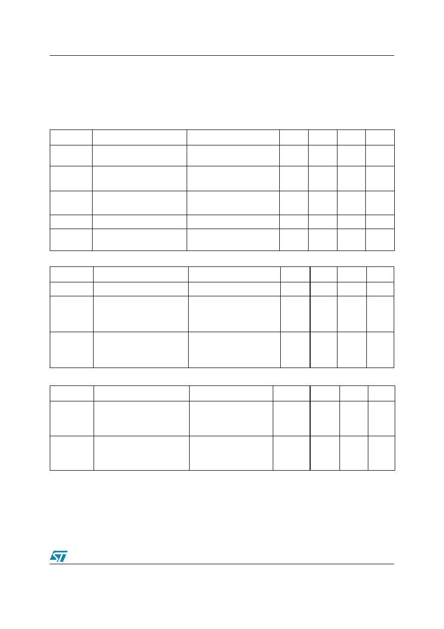
Internal schematic diagram
Type
V
DSS
R
DS(on)
I
D
STD16NF06
60V
<0.070
16A
1
3
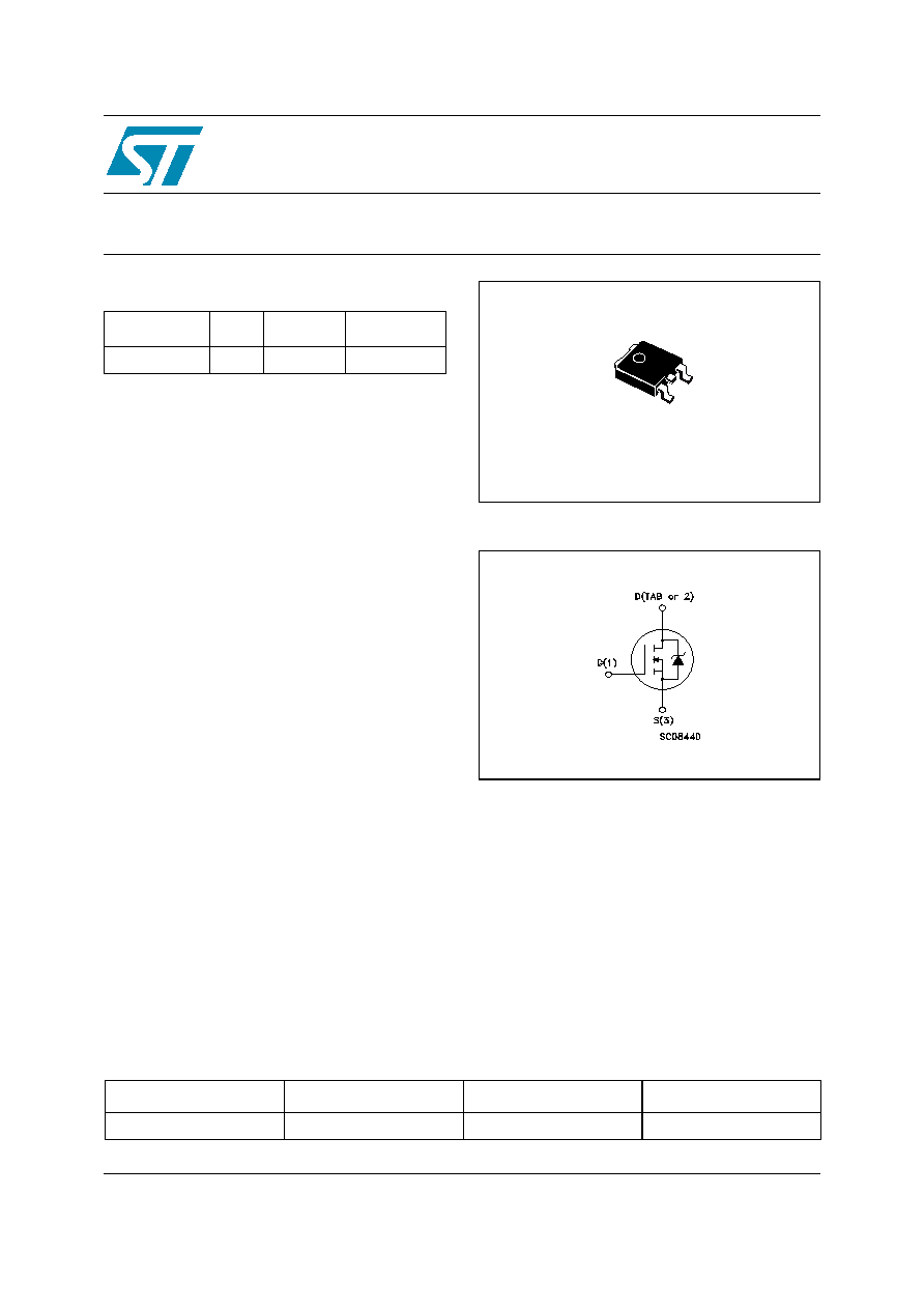
DPAK
TO-252
www.st.com
Order codes
Part Number
Marking
Package
Packaging
STD16NF06T4
D16NF06
TO-252
TAPE & REEL

1 Electrical ratings
STD16NF06
2/11
1 Electrical
ratings
Table 1.
Absolute maximum ratings
Symbol
Parameter
Value
Unit
V
DS
Drain-source Voltage (V
GS
= 0V)
60
V
V
DGR
Drain-gate Voltage (R
GS
= 20 k
)
60
V
V
GS
Gate-Source Voltage
± 20
V
I
D
Drain Current (continuous) at T
C
= 25∞C
16
A
I
D
Drain Current (continuous) at T
C
= 100∞C
11
A
I
DM
Note 4
Drain Current (pulsed)
64
A
P
TOT
Total Dissipation at T
C
= 25∞C
40
W
Derating Factor
0.27
W/∞C
dv/dt
Peak Diode Recovery voltage slope
10.5
V/ns
EAS
Single Pulse Avalanche Energy
178
mJ
T
J
T
stg
Operating Junction Temperature
Storage Temperature
-55 to 175
∞C
Table 2.
Thermal data
R
thJC
Thermal Resistance Junction-case Max
3.75
∞C/W
R
thJA
Thermal Resistance Junction-amb Max
100
∞C/W
T
l
Maximum Lead Temperature For Soldering
Purpose
275
∞C
STD16NF06
2 Electrical characteristics
3/11
2 Electrical
characteristics
( T
CASE
= 25 ∞C unless otherwise specified )
Table 3.
On/off states
Table 5.
Switching times
Symbol
Parameter
Test Conditions
Min.
Typ.
Max.
Unit
V
(BR)DSS
Drain-Source Breakdown
Voltage
I
D
= 250
µ
A V
GS
= 0
60
V
I
DSS
Zero Gate Voltage Drain
Current (V
GS
= 0)
V
DS
= Max Rating
V
DS
= Max Rating T
C
=125∞C
1
10
µA
µA
I
GSS
Gate Body Leakage Current
(V
DS
= 0)
V
GS
= ±20V
±
100
µA
V
GS(th)
Gate Threshold Voltage
V
DS
= V
GS
I
D
= 250µA
2
V
R
DS(on)
Static Drain-Source On
Resistance
V
GS
= 10V I
D
= 8A
0.060
0.070
Table 4.
Dynamic
Symbol
Parameter
Test Conditions
Min.
Typ.
Max.
Unit
g
fs
Note 5
Forward Transconductance
V
DS
= 25V I
D
= 8A
6
S
C
iss
C
oss
C
rss
Input Capacitance
Output Capacitance
Reverse Transfer Capacitance
V
DS
= 15V, f = 1MHz, V
GS
= 0
400
103
41.5
pF
pF
pF
Q
g
Q
gs
Q
gd
Total Gate Charge
Gate-Source Charge
Gate-Drain Charge
V
DD
=30
I
D
= 16A
V
GS
=10V
Figure 14 on page 7
14.1
2.8
5.4
nC
nC
nC
Symbol
Parameter
Test Conditions
Min.
Typ.
Max.
Unit
t
d(on)
t
r
Turn-on Delay Time
Rise Time
V
DD
= 30V, I
D
= 8A,
R
G
= 4.7
,
V
GS
= 10V
Figure 13 on page 7
4
15
ns
ns
t
d(off)
t
f
Off voltage Rise Time
FallTime
V
DD
= 30V, I
D
= 8A,
R
G
= 4.7
,
V
GS
= 10V
Figure 15 on page 7
16
5.5
ns
ns

2 Electrical characteristics
STD16NF06
4/11
Note: 1 Value limited by wire bonding
2 Garanted when external Rg=4.7
and t
f
< t
fmax
.
3 Starting T
J
= 25∞C, I
D
= 19A, V
DD
= 18V
4 Pulse width limited by safe operating area
5 Pulsed: pulse duration = 300µs, duty cycle 1.5%
Table 6.
Source drain diode
Symbol
Parameter
Test Conditions
Min.
Typ.
Max.
Unit
I
SD
I
SDM
Note 4
Source-drain Current
Source-drain Current (pulsed)
16
64
A
A
V
SD
Note 5
Forward on Voltage
I
SD
= 8A V
GS
= 0
1.5
V
t
rr
Q
rr
I
RRM
Reverse Recovery Time
Reverse Recovery Charge
Reverse Recovery Current
I
SD
= 16A, di/dt = 100A/µs,
V
DD
= 20V, T
J
=150∞C
Figure 15 on page 7
49
78
3.2
ns
µ
C
A
STD16NF06
2 Electrical characteristics
5/11
2.1
Electrical chraracteristics (curves)
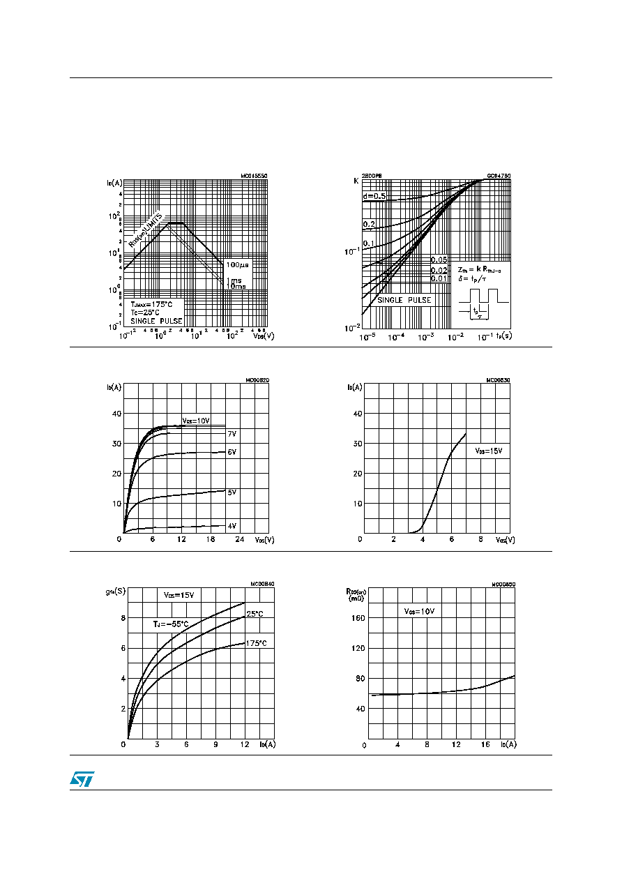
Figure 1.
Safe Operating Area
Figure 2.
Thermal Impedance
Figure 3.
Output Characteristics
Figure 4.
Transfer Characteristics
Figure 5.
Transconductance
Figure 6.
Static Drain-Source on Resistance