DALC112S1
Æ
January 1998 - Ed: 4
IEC 1000-4-2level 3
8 kV (air discharge)
6 kV (contactdischarge)
COMPLIESWITH THE FOLLOWINGSTANDARDS :
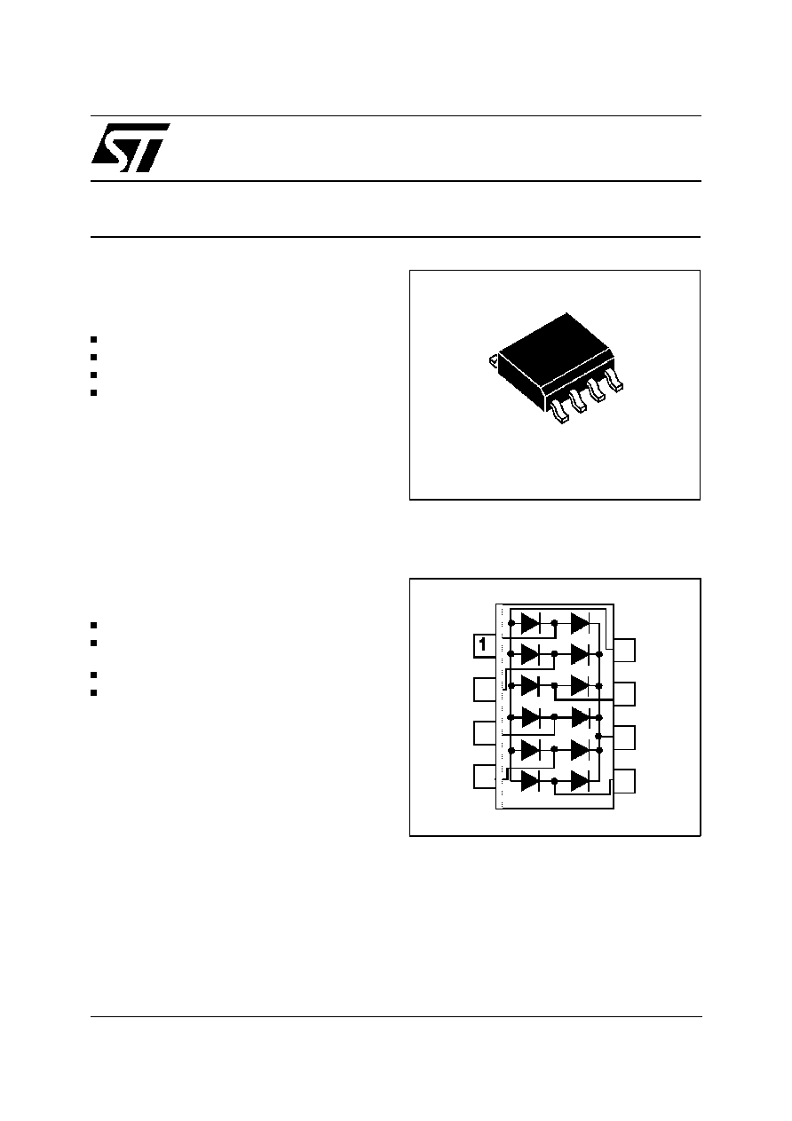
ARRAYOF 12 DIODESFOR ESD PROTECTION.
PEAK REVERSE VOLTAGE V
RRM
= 18V PER
DIODE.
VERYLOWCAPACITANCE PER DIODE: C < 5pF.
VERY LOW LEAKAGE CURRENT : I
R
< 2
µ
A.
FEATURES
SO8
FUNCTIONAL DIAGRAM
I/O 5
I/O 6
I/O 1
I/O 2
I/O 3
I/O 4
REF 1
REF 2
LOW CAPACITANCE DIODE
ARRAY FOR ESD PROTECTION
Application Specific Discretes
A.S.D.
TM
Where ESD protection for high speed datalines is
required :
LAN / WAN equipment
Computer I/O
Graphic video port
Set top box I/O
MAIN APPLICATIONS
ARRAY of 12 diodes configured by cells of 2
diodes, each cell being used to protect signal line
from transient overvoltages by clamping action.
Its very low capacitance allows to protect fast
signals with no distortion. It is particularly suited for
the protection of graphic video ports.
DESCRIPTION
1/3

Symbol
Parameter
Value
Unit
V
RRM
Peak reverse voltage per diode
18
V
T
stg
T
j
Storage temperature range
Maximum junction temperature
-55 to + 150
150
∞
C
∞
C
ABSOLUTE MAXIMUM RATINGS (T
amb
= 25
∞
C).
Symbol
Parameter
Typ.
Max.
Unit
V
F
Forward voltage
I
F
= 50 mA
1.3
V
I
R
Reverse leakage current per diode
V
R
= 15 V
2
µ
A
C
Input capacitance between Line and GND
V
cc
= 5 V, V
RMS
= 30 mV, F = 1 MHz
(see figure 1 below)
7
pF
ELECTRICAL CHARACTERISTICS (T
amb
= 25
∞
C).
TYPICAL APPLICATION
Vcc
DALC112S1
Fig 1 : Input capacitance measurement
+V
CC
connected between REF1 and REF2
Input applied :
Vcc = 5V, V
RMS
= 30 mV, F = 1 MHz
G
I/O
V
CC
REF2
REF1
DALC112S1
2/3

PACKAGE MECHANICAL DATA
SO8 (Plastic)
Information furnished is believed to be accurate and reliable. However, STMicroelectronics assumes no responsibility for the consequences of
use of such information nor for any infringementof patents or other rights of third parties which may result from its use. No license is granted by
implication or otherwise under any patent or patent rights of STMicroelectronics. Specifications mentioned in this publication are subject to
change without notice. This publication supersedes and replaces all informationprevious ly supplied.
STMicroelectronics products are not authorized for use as critical components in life support devices or systems without express written ap-
proval of STMicroelectronics.
©
1998 STMicroelectronics - Printed in Italy - All rights reserved.
STMicroelectronics GROUP OF COMPANIES
Australia - Brazil - Canada - China - France - Germany - Italy - Japan - Korea - Malaysia - Malta - Mexico - Morocco - The
Netherlands - Singapore - Spain - Sweden - Switzerland - Taiwan - Thailand - United Kingdom - U.S.A.
REF.
DIMENSIONS
Millimetres
Inches
Min.
Typ.
Max.
Min.
Typ.
Max.
A
1.75
0.069
a1
0.1
0.25
0.004
0.010
a2
1.65
0.065
b
0.35
0.48
0.014
0.019
b1
0.19
0.25
0.007
0.010
C
0.50
0.020
c1
45
∞
(typ)
D
4.8
5.0
0.189
0.197
E
5.8
6.2
0.228
0.244
e
1.27
0.050
e3
3.81
0.150
F
3.8
4.0
0.15
0.157
L
0.4
1.27
0.016
0.050
M
0.6
0.024
S
8
∞
(max)
Type
Marking
Order Code
Packaging (Base Qty)
DALC112S1
DALC12
DALC112S1
DALC112S1RL
tube (100)
tape & reel (2500)
MARKING
ORDER CODE
RL = tape& reel (2500 pcs).
= tube (100 pcs).
SO8 Package
DALC 1 12 S 1
RL
Version
Diode Array
Low
Capacitance
Nb. of Diodes
PACKAGING : Preferred packaging is tape and reel.
DALC112S1
3/3