 | –≠–ª–µ–∫—Ç—Ä–æ–Ω–Ω—ã–π –∫–æ–º–ø–æ–Ω–µ–Ω—Ç: DB3TG | –°–∫–∞—á–∞—Ç—å:  PDF PDF  ZIP ZIP |

1/4
DB3TG
Æ
October 2001 - Ed: 2A
DIAC
DO-35
s
V
BO
: 32V
s
Low breakover current: 15µA max
s
Breakover voltage range: 30 to 34V
FEATURES
Functioning as a trigger diode with a fixed voltage
reference, the DB3TG can be used in conjunction
with triacs for simplified gate control circuits or as
a starting element in fluorescent lamp ballasts.
DESCRIPTION
Symbol
Parameter
Value
Unit
I
TRM
Repetitive peak on-state current
tp = 20
µ
s
F= 120 Hz
2
A
Tstg
Tj
Storage temperature range
Operating junction temperature range
- 40 to + 125
∞
C
ABSOLUTE MAXIMUM RATINGS (limiting values)
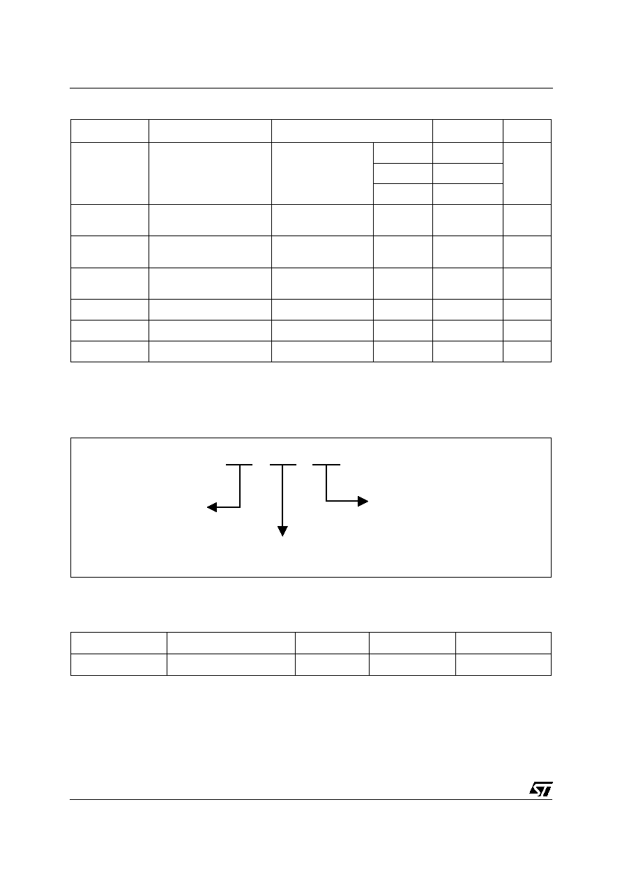
DB3TG
2/4
Symbol
Parameter
Test Conditions
Value
Unit
V
BO
Breakover voltage *
C = 22nF **
MIN.
30
V
TYP.
32
MAX.
34
I V
BO1
- V
BO2
I
Breakover voltage
symmetry
C = 22nF **
MAX.
± 2
V
V
Dynamic breakover
voltage *
V
BO
and V
F
at
10mA
MIN.
9
V
V
O
Output voltage *
see diagram 2
(R=20
)
MIN.
5
V
I
BO
Breakover current *
C = 22nF **
MAX.
15
µ
A
tr
Rise time *
see diagram 3
MAX.
2
µ
s
I
R
Leakage current *
V
R
= 0.5 V
BO
max
MAX.
10
µ
A
* Applicable to both forward and reverse directions.
** Connected in parallel to the device.
ELECTRICAL CHARACTERISTICS (Tj = 25∞C unless otherwise specified)
DB 3
TG
Special V
range
BO
Breakover voltage
3: V
typ = 32V
BO
Diac Series
ORDERING INFORMATION
Part Number
Marking
Weight
Base Quantity
Packing Mode
DB3TG
DB3TG (Blue Body Coat)
0.15 g
5000
Tape & Reel
OTHER INFORMATION
DB3TG
3/4
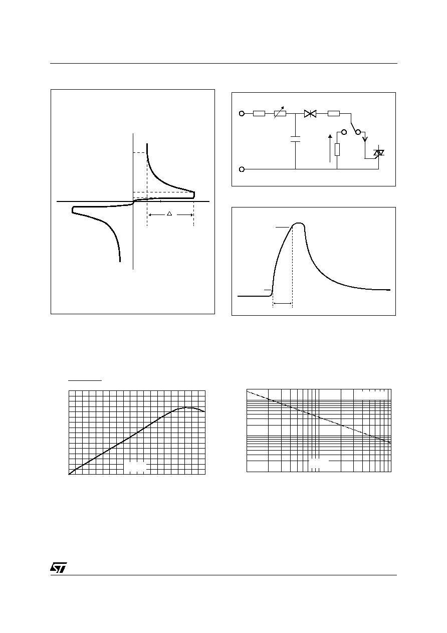
10mA
IBO
I
R
- V
+ V
+ IF
- IF
0,5 VBO
VBO
V
VF
Diagram 1: Voltage - current characteristic curve.
D.U.T
Vo
C=0.1µF
220 V
50 Hz
500 k
10 k
R=20
I
P
Rs=0
T410
Diagram 2: Test circuit.
90 %
l
p
10 %
tr
Diagram 3: Rise time measurement.
25
50
75
100
125
1.08
1.06
1.04
1.02
1.00
VBO [Tj]
VBO [Tj = 25∞C]
Tj (∞C)
Fig. 1: Relative variation of VBO versus junction
temperature (typical values)
1
10
100
0.1
1.0
10.0
20.0
tp(µs)
ITRM(A)
F=120Hz
Tj initial=25∞C
Fig. 2: Repetitive peak pulse current versus pulse
duration (maximum values).
DB3TG
4/4
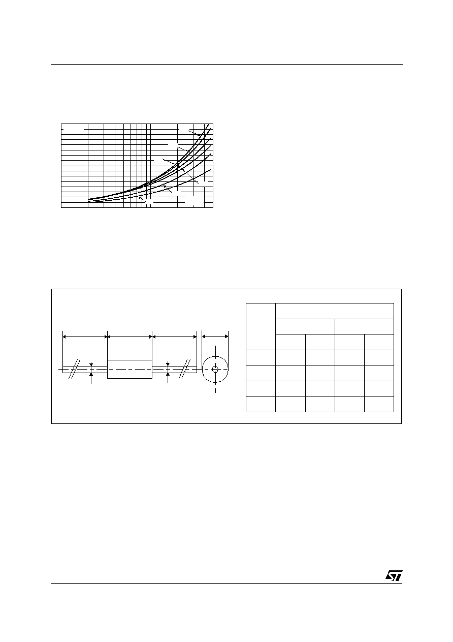
PACKAGE MECHANICAL DATA (in millimeters)
DO-35
REF.
DIMENSIONS
Millimeters
Inches
Min.
Max.
Min.
Max.
A
3.05
4.50
0.120
0.177
B
1.53
2.00
0.060
0.079
C
28.00
1.102
D
0.458
0.558
0.018
0.022
C
A
B
O
/
O
/
D
O
/
D
C
Information furnished is believed to be accurate and reliable. However, STMicroelectronics assumes no responsibility for the consequences of
use of such information nor for any infringement of patents or other rights of third parties which may result from its use. No license is granted by
implication or otherwise under any patent or patent rights of STMicroelectronics. Specifications mentioned in this publication are subject to
change without notice. This publication supersedes and replaces all information previously supplied.
STMicroelectronics products are not authorized for use as critical components in life support devices or systems without express written ap-
proval of STMicroelectronics.
The ST logo is a registered trademark of STMicroelectronics
© 2001 STMicroelectronics - Printed in Italy - All rights reserved.
STMicroelectronics GROUP OF COMPANIES
Australia - Brazil - China - Finland - France - Germany - Hong Kong - India - Italy - Japan - Malaysia
Malta - Morocco - Singapore - Spain - Sweden - Switzerland - United Kingdom - U.S.A.
http://www.st.com
10
20
50
100
200
500
0
5
10
15
20
25
30
35
40
C(nF)
tp(µs)
Tj=25∞C
0
10
22
68
47
33
Fig. 3: Time duration while current pulse is higher
50mA versus C and Rs (typical values).