Æ
1/8
Table 1: Main Product Characteristics
DAMPER
MODUL.
I
F(AV)
6 A
6 A
V
RRM
1500 V
600 V
t
rr
(typ)
150 ns
60 ns
V
F
(typ)
1.1 V
1.0 V
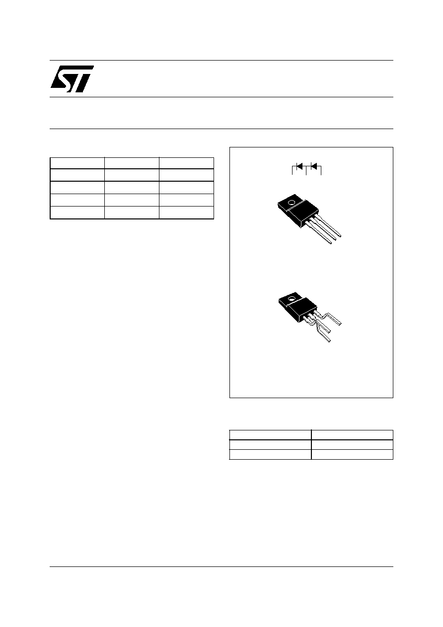
DMV1500SD
DAMPER + MODULATION DIODE FOR VIDEO
1
2
3
TO-220FPAB
DMV1500SDFD
DAMPER
1
2
3
MODULATION
1
2
3
TO-220FPAB FD6
DMV1500SDFD6
(optional)
October 2004
REV. 1
FEATURES AND BENEFITS
Full kit in one package
High breakdown voltage capability
Very fast recovery diode
Specified turn on switching characteristics
Low static and peak forward voltage drop for
low dissipation
Insulated version:
Insulated voltage = 2000 V
RMS
Capacitance = 7 pF
Planar technology allowing high quality and
best electrical characteristics
Outstanding performance of well proven DTV
as damper and new faster Turbo 2 600V
technology as modulation
DESCRIPTION
High voltage semiconductor especially designed
for horizontal deflection stage in standard and high
resolution video display with E/W correction.
The insulated TO-220FPAB package includes
both the DAMPER diode and the MODULATION
diode, thanks to a dedicated design.
Assembled on automated line, it offers very low
dispersion values on insulating and thermal
performanes.
Table 2: Order Codes
Part Number
Marking
DMV1500SDFD
DMV1500SD
DMV1500SDFD6
DMV1500SD

DMV1500SD
2/8
Table 3: Absolute Ratings (limiting values, per diode)
Table 4: Thermal resistances
Table 5: Static Electrical Characteristics
Pulse test:
* tp = 5 ms,
< 2%
** tp = 380 µs,
< 2%
To evaluate the maximum conduction losses of the DAMPER and MODULATION diodes use the following equations :
DAMPER: P = 1.2 x IF(AV) + 0.050 x IF
2
(RMS)
MODULATION: P = 0.89 x IF(AV) + 0.055 x IF
2
(RMS)
Table 6: Recovery Characteristics
Symbol
Parameter
Value
Unit
Damper
Modul.
V
RRM
Repetitive peak reverse voltage
1500
600
V
I
FSM
Surge non repetitive forward current
tp = 10ms sinusoidal
50
50
A
T
stg
Storage temperature range
-40 to +150
∞C
T
j
Maximum operating junction temperature
150
∞C
Symbol
Parameter
Value (max.)
Unit
R
th(j-c)
Junction to case thermal resistance
4
∞C/W
Symbol
Parameter
Test conditions
Value
Unit
T
j
= 25∞C
T
j
= 125∞C
Typ.
Max.
Typ.
Max.
I
R
*
Reverse leakage current
Damper
V
R
= 1500 V
100
100
1000
µA
Modul.
V
R
= 600 V
3
3
30
V
F
**
Forward voltage drop
Damper
I
F
= 6 A
1.2
1.75
1.1
1.5
V
Modul.
I
F
= 6 A
1.15
1.4
1
1.25
Symbol
Parameter
Test conditions
Value
Unit
Damper
Modul.
Typ.
Max.
Typ.
Max.
t
rr
Reverse recovery time
I
F
= 100mA
I
R
=100mA
I
RR
= 10mA
T
j
= 25∞C
1000
2000
250
400
ns
I
F
= 1A
dI
F
/dt = -50 A/µs
V
R
=30V
T
j
= 25∞C
150
250
60
85

DMV1500SD
3/8
Table 7: Turn-On Switching Characteristics
Symbol
Parameter
Test conditions
Value
Unit
Typ.
Max.
t
fr
Forward recovery time
Damper
I
F
= 6 A
dI
F
/dt = 80 A/µs
V
FR
= 3 V
T
j
= 100∞C
350
500
ns
Modul.
I
F
= 6 A
dI
F
/dt = 80 A/µs
V
FR
= 2 V
T
j
= 100∞C
70
125
V
FP
Peak forward voltage
Damper
I
F
= 6 A
dI
F
/dt = 80 A/µs
T
j
= 100∞C
26
36
V
Modul.
I
F
= 6 A
dI
F
/dt = 80 A/µs
T
j
= 100∞C
5
7.5
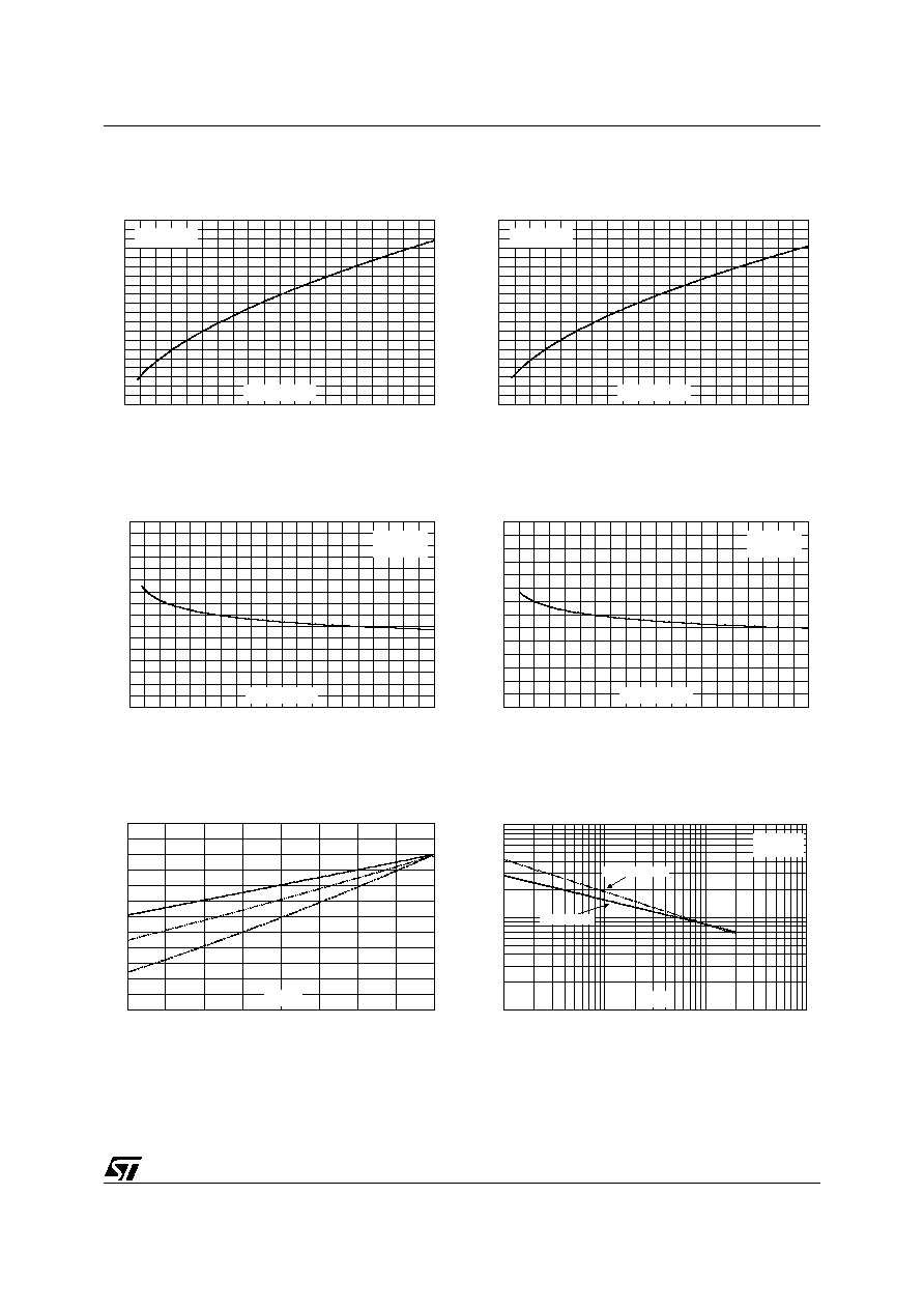
Figure 1: Power dissipation versus peak
forward current (triangular waveform,
=0.45)
(damper diode)
Figure 2: Power dissipation versus peak
forward current (triangular waveform,
=0.45)
(modulation diode)
Figure 3: Average forward current versus
ambient temperature
Figure 4: Forward voltage drop versus forward
current (damper diode)
0.0
0.2
0.4
0.6
0.8
1.0
1.2
1.4
1.6
1.8
2.0
0.0
0.5
1.0
1.5
2.0
2.5
3.0
3.5
4.0
4.5
5.0
5.5
6.0
P
(W)
F(AV)
I (A)
P
0.0
0.2
0.4
0.6
0.8
1.0
1.2
1.4
1.6
0.0
0.5
1.0
1.5
2.0
2.5
3.0
3.5
4.0
4.5
5.0
5.5
6.0
P
(W)
F(AV)
I (A)
P
0
1
2
3
4
5
6
7
0
25
50
75
100
125
150
I
(A)
F(AV)
DAMPER diode
MODULATION diode
T
=tp/T
tp
R
=
th(j-a)
R
th(j-c)
T
(∞C)
amb
0
1
2
3
4
5
6
7
8
9
10
11
12
13
14
15
0.0
0.2
0.4
0.6
0.8
1.0
1.2
1.4
1.6
1.8
2.0
2.2
2.4
I
(A)
FM
V
(V)
FM
T =125∞C
(typical values)
j
T =125∞C
(maximum values)
j
T =25∞C
(maximum values)
j

DMV1500SD
4/8
Figure 5: Forward voltage drop versus forward
current (modulation diode)
Figure 6: Relative variation of thermal
impedance junction to case versus pulse
duration
Figure 7: Reverse recovery charges versus
dI
F
/dt (damper diode)
Figure 8: Reverse recovery charges versus dI
F
/
dt (modulation diode)
Figure 9: Peak reverse recovery current versus
dI
F
/dt (damper diode)
Figure 10: Peak reverse recovery current
versus dI
F
/dt (modulation diode)
0
1
2
3
4
5
6
7
8
9
10
0.2
0.4
0.6
0.8
1.0
1.2
1.4
1.6
1.8
I
(A)
FM
V
(V)
FM
T =125∞C
(typical values)
j
T =125∞C
(maximum values)
j
T =25∞C
(maximum values)
j
0.0
0.1
0.2
0.3
0.4
0.5
0.6
0.7
0.8
0.9
1.0
1.E-03
1.E-02
1.E-01
1.E+00
1.E+01
1.E+02
Z
/R
th(j-c)
th(j-c)
t (s)
p
DAMPER diode
MODULATION diode
Single pulse
0.0
0.5
1.0
1.5
2.0
2.5
3.0
3.5
4.0
0.1
1.0
10.0
100.0
Q (µC)
rr
dI /dt(A/µs)
F
I =
T =125∞C
F
j
I
P
0
50
100
150
200
250
300
0.1
1.0
10.0
100.0
Q (nC)
rr
dI /dt(A/µs)
F
I =
T =125∞C
F
j
I
P
0.0
0.5
1.0
1.5
2.0
2.5
3.0
3.5
4.0
4.5
0.1
1.0
10.0
I
(A)
RM
dI /dt(A/µs)
F
I =
T =125∞C
F
j
I
P
0.0
0.5
1.0
1.5
2.0
2.5
3.0
3.5
4.0
0.1
1.0
10.0
100.0
I
(A)
RM
dI /dt(A/µs)
F
I =
T =125∞C
F
j
I
P
DMV1500SD
5/8
Figure 11: Transient peak forward voltage
versus dI
F
/dt (damper diode, typical values)
Figure 12: Transient peak forward voltage
versus dI
F
/dt (modulation diode, typical values)
Figure 13: Forward recovery time versus dI
F
/dt
(damper diode, typical values)
Figure 14: Forward recovery time versus dI
F
/dt
(modulation diode, typical values)
Figure 15: Relative variation of dynamic
parameters versus junction temperature
Figure 16: Junction capacitance versus
reverse voltage applied (typical values)
0
5
10
15
20
25
30
35
40
45
50
0
20
40
60
80
100
120
140
160
180
200
V
(V)
FP
dI /dt(A/µs)
F
I =
T =100∞C
F
j
I
P
0
1
2
3
4
5
6
7
8
9
10
0
20
40
60
80
100
120
140
160
180
200
V
(V)
FP
dI /dt(A/µs)
F
I =
T =100∞C
F
j
I
P
0
100
200
300
400
500
600
700
800
0
20
40
60
80
100
120
140
160
180
200
t (ns)
fr
I =
T =100∞C
V
F
j
I
=3V
P
FR
dI /dt(A/µs)
F
0
20
40
60
80
100
120
140
0
20
40
60
80
100
120
140
160
180
200
t (ns)
fr
I =
T =100∞C
V
F
j
I
=2V
P
FR
dI /dt(A/µs)
F
0.0
0.2
0.4
0.6
0.8
1.0
1.2
25
50
75
100
125
Q
RR
T (∞C)
j
V
FP
I
RM
I
, V
, Q
[T ]/
RM
FP
RR
j
I
, V
, Q
[T =125∞C]
RM
FP
RR
j
1
10
100
1
10
100
1000
C(pF)
V (V)
R
F=1MHz
V
=30mV
T =25∞C
OSC
RMS
j
DAMPER diode
MODULATION diode