
1/61
September 2002
DSM2190F4V
DSM (Digital Signal Processor System Memory)
For Analog Devices ADSP-2191 DSPs (3.3V Supply)
FEATURES SUMMARY
s
Glueless Connection to DSP
≠ Easily add memory, logic, and I/O to the Exter-
nal Port of ADSP-2191 DSP
s
Dual Flash Memories
≠ Two independent Flash memory arrays for stor-
ing DSP code and data. DSP may access the
two arrays concurrently (read from one while
erasing or writing the other)
≠ 256K x 8 Main Flash memory divided into 8 sec-
tors (32KByte each)
≠ Ample storage for booting DSP code/data
upon reset and subsequent code swaps
≠ Large capacity for data recording
≠ 32K x 8 Secondary Flash memory divided into 4
sectors (8 KByte each). Multiple uses:
≠ Small sector size ideal for small data sets,
and calibration or configuration constants
≠ Store custom start-up code in one or more
sectors and configure DSP to run from exter-
nal memory upon reset (no boot)
≠ Concatenate Secondary Flash with Main
Flash for total of 288 KBytes
≠ Each Flash sector can be write protected.
≠ Built-in programmable address decoding logic
allows mapping individual Flash sectors to any
address boundary
s
Up to 16 Multifunction I/O Pins
≠ Increase total DSP system I/O capability
≠ I/O controlled by DSP software or PLD logic
s
General purpose PLD
≠ Over 3,000 Gates of PLD with 16 macro cells
≠ Use for peripheral glue logic to keypads, control
panel, displays, LCDs, and other devices
≠ Eliminate PLDs and external logic devices
≠ Create state machines, chip selects, simple
shifters and counters, clock dividers, delays
≠ Simple PSDsoft Express
TM
software...Free
s
Operating Range
≠ V
CC
: 3.3V±10%; Temperature: ≠40
o
C to +85
o
C
Figure 1. Packages
s
In-System Programming (ISP) with JTAG
≠ Program entire chip in 10-25 seconds with no in-
volvement of the DSP
≠ Links with ADSP-2191 JTAG debug port
≠ Eliminate sockets for pre-programmed memory
and logic devices
≠ ISP allows efficient manufacturing and product
testing supporting Just-In-Time inventory
≠ Use low-cost FlashLINK
TM
cable with PC
s
Content Security
≠ Programmable Security Bit blocks access of de-
vice programmers and readers
s
Zero-Power Technology
≠ As low as 25
µ
A standby current
s
Packaging
≠ 52-pin PQFP or 52-pin PLCC
s
Flash Memory Speed, Endurance, Retention
≠ 150 ns, 100K cycles, 15 year retention
PLCC52 (K)
PQFP52 (T)

DSM2190F4
2/61
TABLE OF CONTENTS
Summary Description . . . . . . . . . . . . . . . . . . . . . . . . . . . . . . . . . . . . . . . . . . . . . . . . . . . . . . . . . . . . . . 4
Architectural Overview . . . . . . . . . . . . . . . . . . . . . . . . . . . . . . . . . . . . . . . . . . . . . . . . . . . . . . . . . . . . . 6
DSP Address/Data/Control Interface . . . . . . . . . . . . . . . . . . . . . . . . . . . . . . . . . . . . . . . . . . . . . . . . . 6
Main Flash Memory . . . . . . . . . . . . . . . . . . . . . . . . . . . . . . . . . . . . . . . . . . . . . . . . . . . . . . . . . . . . . . 6
Secondary Flash Memory . . . . . . . . . . . . . . . . . . . . . . . . . . . . . . . . . . . . . . . . . . . . . . . . . . . . . . . . . 6
Programmable Logic (PLDs) . . . . . . . . . . . . . . . . . . . . . . . . . . . . . . . . . . . . . . . . . . . . . . . . . . . . . . . 6
Runtime Control Registers . . . . . . . . . . . . . . . . . . . . . . . . . . . . . . . . . . . . . . . . . . . . . . . . . . . . . . . . 7
Memory Page Register . . . . . . . . . . . . . . . . . . . . . . . . . . . . . . . . . . . . . . . . . . . . . . . . . . . . . . . . . . . 7
I/O Ports . . . . . . . . . . . . . . . . . . . . . . . . . . . . . . . . . . . . . . . . . . . . . . . . . . . . . . . . . . . . . . . . . . . . . . 8
JTAG ISP Port . . . . . . . . . . . . . . . . . . . . . . . . . . . . . . . . . . . . . . . . . . . . . . . . . . . . . . . . . . . . . . . . . . 8
Power Management . . . . . . . . . . . . . . . . . . . . . . . . . . . . . . . . . . . . . . . . . . . . . . . . . . . . . . . . . . . . . 8
Security and NVM Sector Protection . . . . . . . . . . . . . . . . . . . . . . . . . . . . . . . . . . . . . . . . . . . . . . . . . 8
Pin Assignments . . . . . . . . . . . . . . . . . . . . . . . . . . . . . . . . . . . . . . . . . . . . . . . . . . . . . . . . . . . . . . . . 8
Typical connections . . . . . . . . . . . . . . . . . . . . . . . . . . . . . . . . . . . . . . . . . . . . . . . . . . . . . . . . . . . . . . 10
Typical Memory Map . . . . . . . . . . . . . . . . . . . . . . . . . . . . . . . . . . . . . . . . . . . . . . . . . . . . . . . . . . . . . . 12
Specifying the Memory Map with PSDsoft ExpressTM . . . . . . . . . . . . . . . . . . . . . . . . . . . . . . . . . . 14
Runtime control register definition . . . . . . . . . . . . . . . . . . . . . . . . . . . . . . . . . . . . . . . . . . . . . . . . . . 15
Detailed Operation . . . . . . . . . . . . . . . . . . . . . . . . . . . . . . . . . . . . . . . . . . . . . . . . . . . . . . . . . . . . . . . . 16
Flash Memories . . . . . . . . . . . . . . . . . . . . . . . . . . . . . . . . . . . . . . . . . . . . . . . . . . . . . . . . . . . . . . . . 16
Instruction Sequences . . . . . . . . . . . . . . . . . . . . . . . . . . . . . . . . . . . . . . . . . . . . . . . . . . . . . . . . . . . 18
Reading Flash Memory . . . . . . . . . . . . . . . . . . . . . . . . . . . . . . . . . . . . . . . . . . . . . . . . . . . . . . . . . . 18
Programming Flash Memory . . . . . . . . . . . . . . . . . . . . . . . . . . . . . . . . . . . . . . . . . . . . . . . . . . . . . . 19
Erasing Flash Memory. . . . . . . . . . . . . . . . . . . . . . . . . . . . . . . . . . . . . . . . . . . . . . . . . . . . . . . . . . . 21
Flash Memory Sector Protect. . . . . . . . . . . . . . . . . . . . . . . . . . . . . . . . . . . . . . . . . . . . . . . . . . . . . . 22
DSM Security Bit . . . . . . . . . . . . . . . . . . . . . . . . . . . . . . . . . . . . . . . . . . . . . . . . . . . . . . . . . . . . . . . 23
Reset Flash . . . . . . . . . . . . . . . . . . . . . . . . . . . . . . . . . . . . . . . . . . . . . . . . . . . . . . . . . . . . . . . . . . . 23
Page Register . . . . . . . . . . . . . . . . . . . . . . . . . . . . . . . . . . . . . . . . . . . . . . . . . . . . . . . . . . . . . . . . . 23
PLDs . . . . . . . . . . . . . . . . . . . . . . . . . . . . . . . . . . . . . . . . . . . . . . . . . . . . . . . . . . . . . . . . . . . . . . . . 23
Decode PLD (DPLD). . . . . . . . . . . . . . . . . . . . . . . . . . . . . . . . . . . . . . . . . . . . . . . . . . . . . . . . . . . . . . . 25

3/61
DSM2190F4
Complex PLD (CPLD) . . . . . . . . . . . . . . . . . . . . . . . . . . . . . . . . . . . . . . . . . . . . . . . . . . . . . . . . . . . . . 26
DSP Bus Interface . . . . . . . . . . . . . . . . . . . . . . . . . . . . . . . . . . . . . . . . . . . . . . . . . . . . . . . . . . . . . . 30
I/O Ports . . . . . . . . . . . . . . . . . . . . . . . . . . . . . . . . . . . . . . . . . . . . . . . . . . . . . . . . . . . . . . . . . . . . . 30
Port Operating Modes . . . . . . . . . . . . . . . . . . . . . . . . . . . . . . . . . . . . . . . . . . . . . . . . . . . . . . . . . . . 31
Port B ≠ Functionality and Structure . . . . . . . . . . . . . . . . . . . . . . . . . . . . . . . . . . . . . . . . . . . . . . . . 33
Port C ≠ Functionality and Structure . . . . . . . . . . . . . . . . . . . . . . . . . . . . . . . . . . . . . . . . . . . . . . . . 34
Port D ≠ Functionality and Structure . . . . . . . . . . . . . . . . . . . . . . . . . . . . . . . . . . . . . . . . . . . . . . . . 35
Power Management . . . . . . . . . . . . . . . . . . . . . . . . . . . . . . . . . . . . . . . . . . . . . . . . . . . . . . . . . . . . . . . 37
PLD Power Management . . . . . . . . . . . . . . . . . . . . . . . . . . . . . . . . . . . . . . . . . . . . . . . . . . . . . . . . 38
PSD Chip Select Input (CSI, PD2) . . . . . . . . . . . . . . . . . . . . . . . . . . . . . . . . . . . . . . . . . . . . . . . . . 38
Power On Reset, Warm Reset, Power-down . . . . . . . . . . . . . . . . . . . . . . . . . . . . . . . . . . . . . . . . . 39
Programming In-Circuit using JTAG ISP . . . . . . . . . . . . . . . . . . . . . . . . . . . . . . . . . . . . . . . . . . . . . . 40
AC/DC Parameters . . . . . . . . . . . . . . . . . . . . . . . . . . . . . . . . . . . . . . . . . . . . . . . . . . . . . . . . . . . . . . . . 42
Table: Absolute Maximum Ratings . . . . . . . . . . . . . . . . . . . . . . . . . . . . . . . . . . . . . . . . . . . . . . . . . 43
Table: Operating Conditions . . . . . . . . . . . . . . . . . . . . . . . . . . . . . . . . . . . . . . . . . . . . . . . . . . . . . . 44
Table: DC Characteristics . . . . . . . . . . . . . . . . . . . . . . . . . . . . . . . . . . . . . . . . . . . . . . . . . . . . . . . . 46
Table: CPLD Combinatorial Timing . . . . . . . . . . . . . . . . . . . . . . . . . . . . . . . . . . . . . . . . . . . . . . . . . 47
Table: CPLD Macrocell Synchronous Clock Mode Timing . . . . . . . . . . . . . . . . . . . . . . . . . . . . . . . 48
Table: CPLD Macrocell Asynchronous Clock Mode Timing . . . . . . . . . . . . . . . . . . . . . . . . . . . . . . 48
Table: Input Macrocell Timing . . . . . . . . . . . . . . . . . . . . . . . . . . . . . . . . . . . . . . . . . . . . . . . . . . . . . 50
Table: Read Timing . . . . . . . . . . . . . . . . . . . . . . . . . . . . . . . . . . . . . . . . . . . . . . . . . . . . . . . . . . . . . 51
Table: Write Timing . . . . . . . . . . . . . . . . . . . . . . . . . . . . . . . . . . . . . . . . . . . . . . . . . . . . . . . . . . . . . 52
Table: Flash Memory Program, Write and Erase Times . . . . . . . . . . . . . . . . . . . . . . . . . . . . . . . . . 53
Table: Reset (Reset) Timing . . . . . . . . . . . . . . . . . . . . . . . . . . . . . . . . . . . . . . . . . . . . . . . . . . . . . . 53
Table: ISC Timing . . . . . . . . . . . . . . . . . . . . . . . . . . . . . . . . . . . . . . . . . . . . . . . . . . . . . . . . . . . . . . 54
Package Mechanical . . . . . . . . . . . . . . . . . . . . . . . . . . . . . . . . . . . . . . . . . . . . . . . . . . . . . . . . . . . . . . 55
Table: PLCC52 - 52 lead Plastic Leaded Chip Carrier, rectangular . . . . . . . . . . . . . . . . . . . . . . . . 55
Table: Assignments ≠ PLCC52 . . . . . . . . . . . . . . . . . . . . . . . . . . . . . . . . . . . . . . . . . . . . . . . . . . . . 56
Table: PQFP52 - 52 lead Plastic Quad Flatpack . . . . . . . . . . . . . . . . . . . . . . . . . . . . . . . . . . . . . . . 57
Table: Pin Assignments ≠ PQFP52 . . . . . . . . . . . . . . . . . . . . . . . . . . . . . . . . . . . . . . . . . . . . . . . . . 58
Table: Ordering Information Scheme . . . . . . . . . . . . . . . . . . . . . . . . . . . . . . . . . . . . . . . . . . . . . . . 59

DSM2190F4
4/61
SUMMARY DESCRIPTION
The DSM2190F4 is a system memory device for
use with the Analog Devices ADSP-2191 DSP.
DSM means Digital signal processor System
Memory. A DSM device brings In-System Pro-
grammable (ISP) Flash memory, parameter stor-
age, programmable logic, and additional I/O to
DSP systems. The result is a simple and flexible
two-chip solution for DSP designs. DSM devices
provide the flexibility of Flash memory and smart
JTAG programming techniques for both manufac-
turing and the field. On-chip integrated memory
decode logic makes it easy to map dual banks of
Flash memory to the ADSP-2191 in a variety of
ways for bootloading, code execution, data re-
cording, code swapping, and parameter storage.
JTAG ISP reduces development time, simplifies
manufacturing flow, and lowers the cost of field up-
grades. The JTAG ISP interface eliminates the
need for sockets and pre-programmed memory
and logic devices. For manufacturing, end prod-
ucts may be assembled with a blank DSM device
soldered to the circuit board and programmed at
the end of the manufacturing line in 10 to 25 sec-
onds with no involvement of the DSP. This allows
efficient means to test product and manage inven-
tory by rapidly programming test code, then appli-
cation code as determined by inventory
requirements (Just-In Time inventory). Additional-
ly, JTAG ISP reduces development time by turning
fast iterations of DSP code in the lab. Code up-
dates in the field require no disassembly of prod-
uct. The FlashLINK
TM
JTAG programming cable
costs $59 USD and plugs into any PC or note-
book parallel port.
In addition to ISP Flash memory, DSM devices
add programmable logic (PLD) and up to 16 con-
figurable I/O pins to the DSP system. The state of
each I/O pin can be driven by DSP software or
PLD logic. PLD and I/O configuration are program-
mable by JTAG ISP, just like the Flash memory.
The PLD consists of more than 3000 gates and
has 16 macro cell registers. Common uses for the
PLD include chip selects for external devices,
state-machines, simple shifters and counters, key-
pad and control panel interfaces, clock dividers,
handshake delay, multiplexers, etc. This elimi-
nates the need for small external PLDs and logic
devices. Configuration of PLD, I/O, and Flash
memory mapping are easily entered in a point-
and-click environment using the software develop-
ment tool, PSDsoft Express
TM
. This software is
available at no charge from
www.st.com/psm
.
Figure 2. System Block Diagram, Two-Chip Solution
ADDR
& DE
CO
DE
LO
GI
C
PRIMARY
FLASH MEMORY
256K X 8
16 MACROCELL PLD
I/O CONTROL
POWER MANAGEMENT
CONTENT SECURITY
8 I/O
PORTS
8 I/O
PORTS
JTAG
ISP TO
ALL
AREAS
I/O
B
U
S
22 ADDRESS
8 DATA
WR, RD, BMS, MSx, IOMS
I/O, PLD, CHIP SELECTS
I/O, PLD, CHIP SEL
DSM2190F4
DSP SYSTEM MEMORY
ANALOG
DEVICES
DSP
ADSP-2191
SERIAL
DEVICE
16 FLAGS
SERIAL
DEVICE
SERIAL
DEVICE
UART
DEVICE
JTAG ISP
JTAG DEBUG
HOST
MCU
TIMER/
CAPTURE
SECONDARY
FLASH MEMORY
32K X 8
AI04959B
5/61
DSM2190F4
The two-chip combination of a DSP and a DSM
device is ideal for systems which have limitations
on size, EMI levels, and power consumption. DSM
memory and logic are "zero-power", meaning they
automatically go to standby between memory ac-
cesses or logic input changes, producing low ac-
tive and standby current consumption, which is
ideal for battery powered products.
A programmable security bit in the DSM protects
its contents from unauthorized viewing and copy-
ing. When set, the security bit will block access of
programming devices (JTAG or others) to the
DSM Flash memories and PLD configuration. The
only way to defeat the security bit is to erase the
entire DSM device, after which the device is blank
and may be used again. The DSP will always have
access to Flash memory contents through the 8-bit
data port even while the security bit is set.
Table 1. DSM2190F4V DSP Memory System Devices
Table 2. Compatible Analog Devices DSP
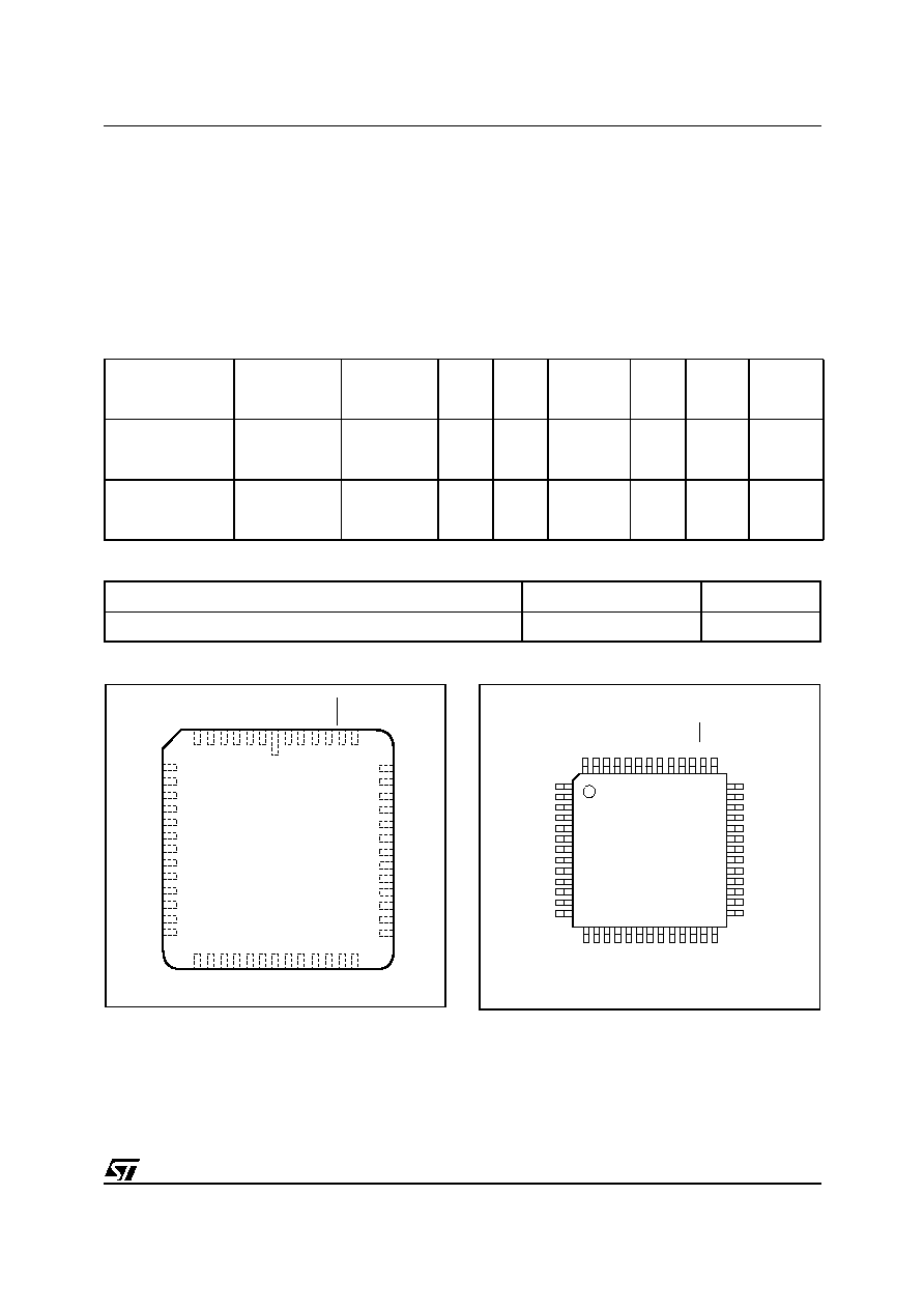
Figure 3. PLCC Connections
Figure 4. PQFP Connections
Part Number
Main Flash
Memory
Secondary
Flash
Memory
PLD
I/O
Ports
V
CC
and I/O
Mem
Speed
Package
Operating
Temp
DSM2190F4VV-
15T6
256KBytes =
8 sectors x
32KByte
32KBytes =
4 sectors x
8KByte
16
macro
-cells
Up to
16
3.3V ±10%
150 ns
52-pin
PQFP
≠40
o
C to
+85
o
C
DSM2190F4VV-
15K6
256KBytes =
8 sectors x
32KByte
32KBytes =
4 sectors x
8KByte
16
macro
-cells
Up to
16
3.3V ±10%
150 ns
52-pin
PLCC
≠40
o
C to
+85
o
C
DSP Part Number
Operating Voltage, V
CC
I/O Capability
ADSP-2191M
2.5V
2.5 - 3.6V
PB0
PB1
PB2
PB3
PB4
PB5
GND
PB6
PB7
CNTL1
CNTL2
RESET
CNTL0
PA
7
PA
6
PA
5
PA
4
PA
3
GND
PA
2
PA
1
PA
0
AD0
AD1
AD2
AD3
AD15
AD14
AD13
AD12
AD11
AD10
AD9
AD8
VCC
AD7
AD6
AD5
AD4
PD2
PD1
PD0
PC7
PC6
PC5
PC4
VCC
GND
PC3
PC2
PC1
PC0
8
9
10
11
12
13
14
15
16
17
18
19
20
46
45
44
43
42
41
40
39
38
37
36
35
34
21
22
23
24
25
26
27
28
29
30
31
32
33
47
48
49
50
51
52
1
2
3
4
5
6
7
AI02857
39 AD15
38 AD14
37 AD13
36 AD12
35 AD11
34 AD10
33 AD9
32 AD8
31 V
CC
30 AD7
29 AD6
28 AD5
27 AD4
PD2
PD1
PD0
PC7
PC6
PC5
PC4
V
CC
GND
PC3
PC2
PC1
PC0
1
2
3
4
5
6
7
8
9
10
11
12
13
52
51
50
49
48
47
46
45
44
43
42
41
40
PB0
PB1
PB2
PB3
PB4
PB5
GND
PB6
PB7
CNTL1
CNTL2
RESET
CNTLO
14
15
16
17
18
19
20
21
22
23
24
25
26
PA7
PA6
PA5
PA4
PA3
GND
PA2
PA1
PA0
AD0
AD1
AD2
AD3
AI02858