 | –≠–ª–µ–∫—Ç—Ä–æ–Ω–Ω—ã–π –∫–æ–º–ø–æ–Ω–µ–Ω—Ç: EF6805P2 | –°–∫–∞—á–∞—Ç—å:  PDF PDF  ZIP ZIP |
EF6805U3
March 1989
8-BIT MICROCOMPUTER UNIT
.
32 TTL/CMOS COMPATIBLE I/O LINES
.
24 BIDIRECTIONAL (8 lines are LED compati-
ble)
.
8 INPUT-ONLY
.
3776 BYTES OF USER ROM
.
112 BYTES OF RAM
.
SELF-CHECK MODE
.
ZERO-CROSSING DETECT/INTERRUPT
.
INTERNAL 8-BIT TIMER WITH 7-BIT SOFT-
WARE PROGRAMMABLE PRESCALER AND
CLOCK SOURCE
.
5V SINGLE SUPPLY
SOFTWARE FEATURES
.
10 POWERFUL ADDRESSING MODES
.
BYTE EFFICIENT INSTRUCTION SET WITH
TRUE BIT MANIPULATION, BIT TEST, AND
BRANCH INSTRUCTIONS
.
SINGLE
INSTRUCTION
MEMORY
EXA-
MINE/CHANGE
.
POWERFUL INDEXED ADDRESSING FOR
TABLES
.
FULL SET OF CONDITIONAL BRANCHES
.
MEMORY USABLE AS REGISTER/FLAGS
.
COMPLETE DEVELOPMENT SYSTEM SUP-
PORT ON INICE
USER SELECTABLE OPTIONS
.
8 BIDIRECTIONAL I/O LINES WITH TTL OR
TTL/CMOS INTERFACE OPTION
.
8 BIDIRECTIONAL I/O LINES WITH TTL OR O-
PEN-DRAIN INTERFACE OPTION
.
CRYSTAL OR LOW-COST RESISTOR OSCIL-
LATOR OPTION
.
LOW VOLTAGE INHIBIT OPTION
.
VECTORED INTERRUPTS : TIMER, SOFT-
WARE, AND EXTERNAL
.
USER CALLABLE SELF-CHECK SUBROU-
TINES
HARDWARE FEATURES
DESCRIPTION
The EF6805U3 Microcomputer Unit (MCU) is a
member of the 6805 Family of low-cost single-chip
Microcomputers. The 8-bit microcomputer contains
a CPU, on-chip CLOCK, ROM, RAM, I/O, and TI-
MER. It is designed for the user who needs an eco-
nomical microcomputer with the proven capabilities
of the 6800-based instruction set. A comparison of
the key features of several members of the 6805 Fa-
mily of Microcomputers is shown at the end of this
data sheet. The following are some of the hardware
and software highlights of the EF6805U3 MCU.
1
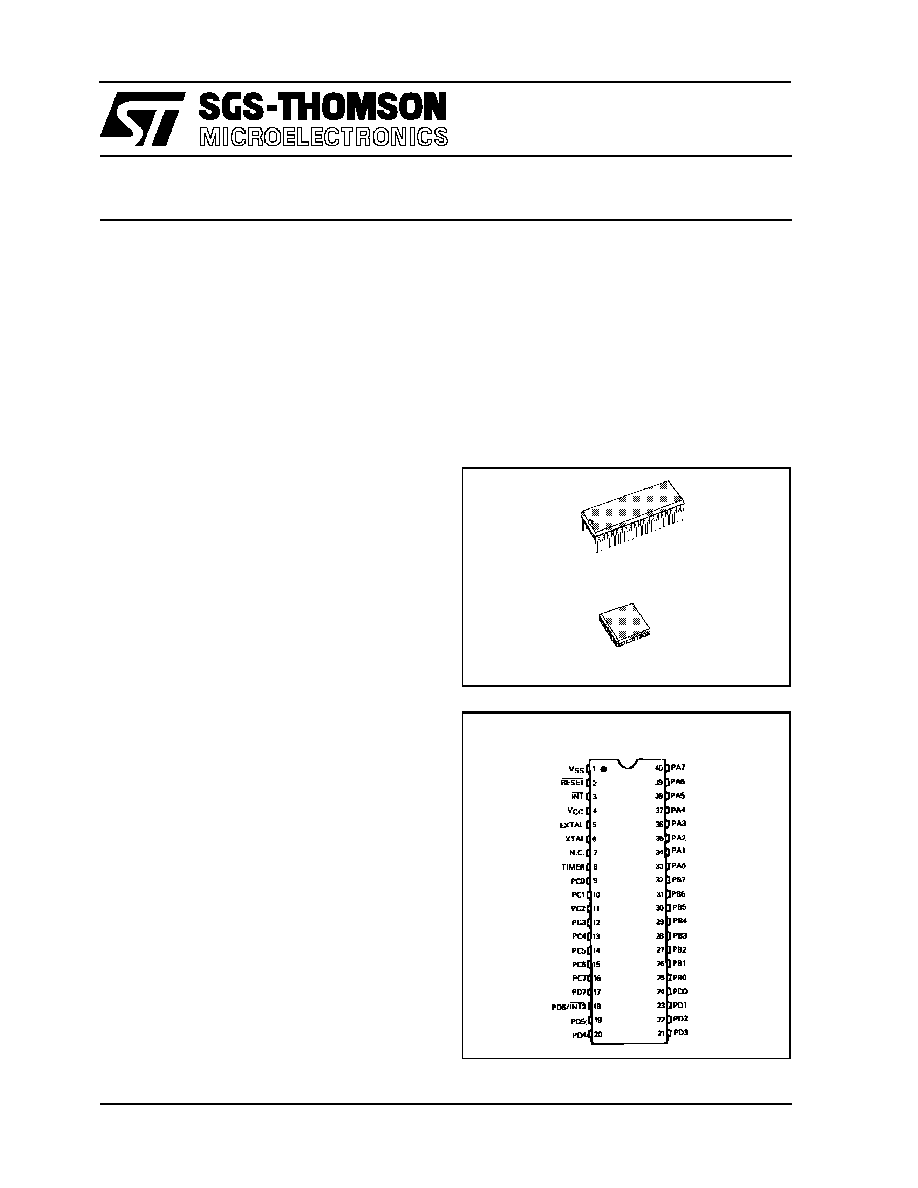
PIN CONNECTIONS
FN
(PLCC 44)
P
(PDIP40)
1/31
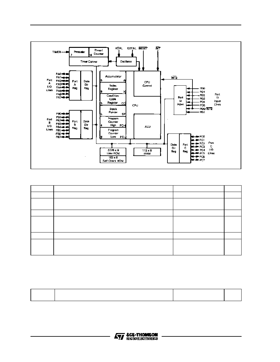
Figure 1 : EF6805U3 HMOS Microcomputer Block Diagram.
ABSOLUTE MAXIMUM RATINGS
Symbol
Parameter
Value
Unit
V
CC
Supply Voltage
≠ 0.3 to + 7.0
V
V
in
Input Voltage (except TIMER in self-check mode and
open-drain inputs)
≠ 0.3 to + 7.0
V
V
in
Input Voltage (open-drain pins, TIMER pin in self-check mode)
≠ 0.3 to + 15.0
V
T
A
Operating Temperature Range
V Suf fix
T Suf fix
(T
L
to T
H
)
0 to + 70
≠ 40 to + 85
≠ 40 to + 105
∞
C
T
s t g
Storage Temperature Range
≠ 55 to + 150
∞
C
T
j
Junction Temperature
Plastic Package
PLCC
150
150
∞
C
This device contains circuitry to protect the inputs against damage due to high static voltages or electrical fields, however, it is advised
that normal precautions be taken to avoid application of any voltage higher than maximum rated voltages to this high impedance circuit.
For proper operation it is recommended that V
in
and V
out
be constrained to the range V
SS
(V
in
or V
out
) V
CC
. Reliability of operation is en-
hanced if unused inputs except EXTAL are tied to an appropriate logic voltage level (e.g., either V
SS
or V
CC
).
THERMAL DATA
J A
Thermal Resistance
Plastic
PLCC
50
80
∞
C/W
EF6805U3
2/31

POWER CONSIDERATIONS
The average chip-junction temperature, T
J
, in C can
be obtained from :
T
J
= T
A
+ (P
D
.J
A
) (1)
Where :
T
A
= Ambient Temperature, C
J
A
= Package Thermal Resistance, Junction-to-Am-
bient, C/W
P
D
= P
INT
+ P
PORT
P
INT
= I
CC
x V
CC
, Watts - Chip Internal Power
P
PORT
= Port Power Dissipation, Watts - User De-
termined
For most applications P
PORT
P
INT
and can be ne-
glected. P
PORT
may become significant if the device
is configured to drive Darlington bases or sink LED
loads.
An approximate relationship between P
D
and T
J
(if
P
PORT
is neglected) is :
P
D
= K + (T
J
+ 273C) (2)
Solving equations 1 and 2 for K gives :
K = P
D
.(T
A
+ 273C) + J
A
.P
D
2
(3)
Where K is a constant pertaining to the particular
part. K can be determined from equation 3 by mea-
suring P
D
(at equilibrium) for a known T
A
. Using this
value of K the values of P
D
and T
J
can be obtained
by solving equations (1) and (2) iteratively for any
value of T
A
.
ELECTRICAL CHARACTERISTICS(V
CC
= + 5.25Vdc
±
0.5Vdc, V
S S
= 0Vdc, T
A
= T
L
to T
H
unless
otherwise noted)
Symbol
Parameter
Min.
Typ.
Max.
Unit
V
IH
Input High Voltage
RESET (4.75
V
CC
5.75)
(V
CC
< 4.75)
INT (4.75
V
CC
5.75)
(V
CC
< 4.75)
All Other (except timer)
4.0
V
CC
≠ 0.5
4.0
V
CC
≠ 0.5
2.0
∑
∑
V
CC
V
CC
V
CC
V
CC
V
CC
V
V
IH
Input High Voltage Timer
Timer Mode
Self-check Mode
2.0
9.0
10.0
V
CC
+ 1.0
15.0
V
V
IL
Input Low Voltage
RESET
INT
All Other
V
SS
V
SS
V
SS
∑
0.8
1.5
0.8
V
V
IRE S +
V
IRE S ≠
RESET Hystereris Voltages (see figures 10, 11 and 12)
"Out of Reset"
"Into Reset"
2.1
0.8
4.0
2.0
V
V
IN T
INT Zero Crossing Input Voltage, Through a
Capacitor
2
4
V
ac p -p
P
D
Power Dissipation - (no port loading, V
CC
= 5.75V)
T
A
= 0
∞
C
T
A
= ≠ 40
∞
C
520
580
740
800
mW
C
in
Input Capacitance
EXTAL
All Other
25
10
pF
V
L V R
Low Voltage Recover
4.75
V
VL
V I
Low Voltage Inhibit
2.75
3.75
4.70
V
I
in
Input Current
TIMER (V
i n
= 0.4V)
INT (V
in
= 2.4V to V
CC
)
EXTAL (V
i n
= 2.4V to V
CC
- crystal option)
(V
in
= 0.4V - crystal option)
RESET (V
i n
= 0.8V) - External Capacitor Charging
Current
≠ 40.0
20
20
50
10
≠ 1600
≠ 40
µ
A
* Due to internal biasing this input (when unused) floats to approximately 2.2V.
EF6805U3
3/31

SWITCHING CHARACTERISTICS
(V
C C
= + 5.25Vdc
±
0.5Vdc, V
S S
= 0Vdc, T
A
= T
L
to T
H
unless otherwise noted)
Symbol
Parameter
Min.
Typ.
Max.
Unit
f
o s c
Oscillator Frequency
0.4
4.2
MHz
t
c yc
Cycle Time (4/f
o s c
)
0.95
10
µ
s
t
WL
, t
WH
INT, INT2, and TIMER Pulse Width (see interrupt
section)
t
c y c
+ 250
ns
t
RWL
RESET Pulse Width
t
c y c
+ 250
ns
f
IN T
INT Zero-crossing Detection Input Frequency
0.03
1
kHz
External Clock Input Duty Cycle (EXTAL)
40
50
60
%
Crystal Oscillator Start-up Time*
100
ms
PORT ELECTRICAL CHARACTERISTICS
(V
C C
= + 5.25Vdc
±
0.5Vdc, V
S S
= 0Vdc, T
A
= T
L
to T
H
unless otherwise noted)
PORT A WITH CMOS DRIVE ENABLED
Symbol
Parameter
Min.
Typ.
Max.
Unit
V
O L
Output Low Voltage (I
L o ad
= 1.6mA)
0.4
V
V
O H
Output High Voltage
I
L o ad
= ≠ 100
µ
A
I
L o ad
= ≠ 10
µ
A
2.4
V
CC
≠ 1.0
V
V
IH
Input High Voltage (I
L o ad
= ≠ 300
µ
A max.)
2.0
V
CC
V
V
IL
Input Low Voltage (I
L o ad
= ≠ 500
µ
A max.)
V
SS
0.8
V
I
IH
High Z State Input Current (V
i n
= 2.0V to V
CC
)
≠ 300
µ
A
I
IL
High Z State Input Current (V
i n
= 0.4V)
≠ 500
µ
A
PORT B
Symbol
Parameter
Min.
Typ.
Max.
Unit
V
O L
Output Low Voltage
I
L o ad
= 3.2mA
I
L o ad
= 10mA (sink)
0.4
1.0
V
V
O H
Output High Voltage I
L o ad
= ≠ 200
µ
A
2.4
V
I
O H
Darlington Current Drive (source) V
O
= 1.5V
≠ 1.0
≠ 10
mA
V
IH
Input High Voltage
2.0
V
CC
V
V
IL
Input Low Voltage
V
SS
0.8
V
I
TS I
High Z State Input Current
< 2
10
µ
A
PORT C AND PORT A WITH CMOS DRIVE DISABLED
Symbol
Parameter
Min.
Typ.
Max.
Unit
V
O L
Output Low Voltage I
L o ad
= 1.6mA
0.4
V
V
O H
Output High Voltage I
L o ad
= ≠ 100
µ
A
2.4
V
V
IH
Input High Voltage
2.0
V
CC
V
V
IL
Input Low Voltage
V
SS
0.8
V
I
TS I
High Z State Input Current
< 2
10
µ
s
EF6805U3
4/31

Figure 2 : TTL Equivalent Test Load (port B).
Figure 3 : CMOS Equivalent Test Load (port A).
Figure 4 : TTL Equivalent Test Load (port A
andC).
Figure 5 : Open-drain Equivalent Test Load (port
C).
SIGNAL DESCRIPTION
The input and output signals for the MCU, shown in
figure 1, are described in the following paragraphs.
V
CC
AND V
SS
- Power is supplied to the MCU using
these two pins. V
CC
is power and V
SS
is the ground
connection.
INT - This pin provides the capability for asynchro-
nously applying an external interrupt to the MCU.
Refer to Interrupts Section for additional informa-
tion.
XTAL AND EXTAL - These pins provide control in-
put for theon-chip clock oscillator circuit. A crystal,
a resistor, or an external signal, depending on user
selectable manufacturing mask option, can be
connected to these pins to provide a system clock
with various degrees of stability/cost tradeoffs. Lead
length and stray capacitance on these two pins
should be minimized. Refer to Internal Clock Gen-
erator Options Section for recommendations about
these inputs.
NOTE : Pin 7 in DIL package/pin 8 in PLCC
package is connected to internal protection.
TIMER - The pin allows an external input to be used
to control the internal timer circuitry and also to ini-
tiate the self test program. Refer to Timer Section for
additional information about the timer circuitry.
RESET - This pin allows resetting of the MCU at
times other than the automatic resetting capability
already in the MCU. The MCU can be reset by pul-
ling RESET low. Refer to Resets Section for addi-
tional information.
EF6805U3
5/31