Rev 1
September 2005
1/8
8
EMIF07-LCD02F3
IPADTM
7 line EMI filter and ESD protection for LCD and cameras
Main product characteristics:
Where EMI filtering in ESD sensitive equipment is
required :
LCD for Mobile phones
Computers and printers
Communication systems
MCU Boards
Description
The EMIF07-LCD02F3 is a 7 line highly integrated
devices designed to suppress EMI/RFI noise in all
systems subjected to electromagnetic
interferences. The EMIF07 flip-chip packaging
means the package size is equal to the die size.
This filter includes ESD protection circuitry, which
prevents damage to the application when
subjected to ESD surges up 15 kV.
Benefits
Lead free package
EMI symmetrical (I/O) low-pass filter
High efficiency in EMI filtering
400 µm pitch
Compatible with high speed data rate
Very low PCB space consuming: < 3.1 mm
2
Very thin package: 0.6 mm
High efficiency in ESD suppression
High reliability offered by monolithic integration
High reducing of parasitic elements through
integration and wafer level packaging
Order Code
TM: IPAD is a trademark of STMicroelectronics
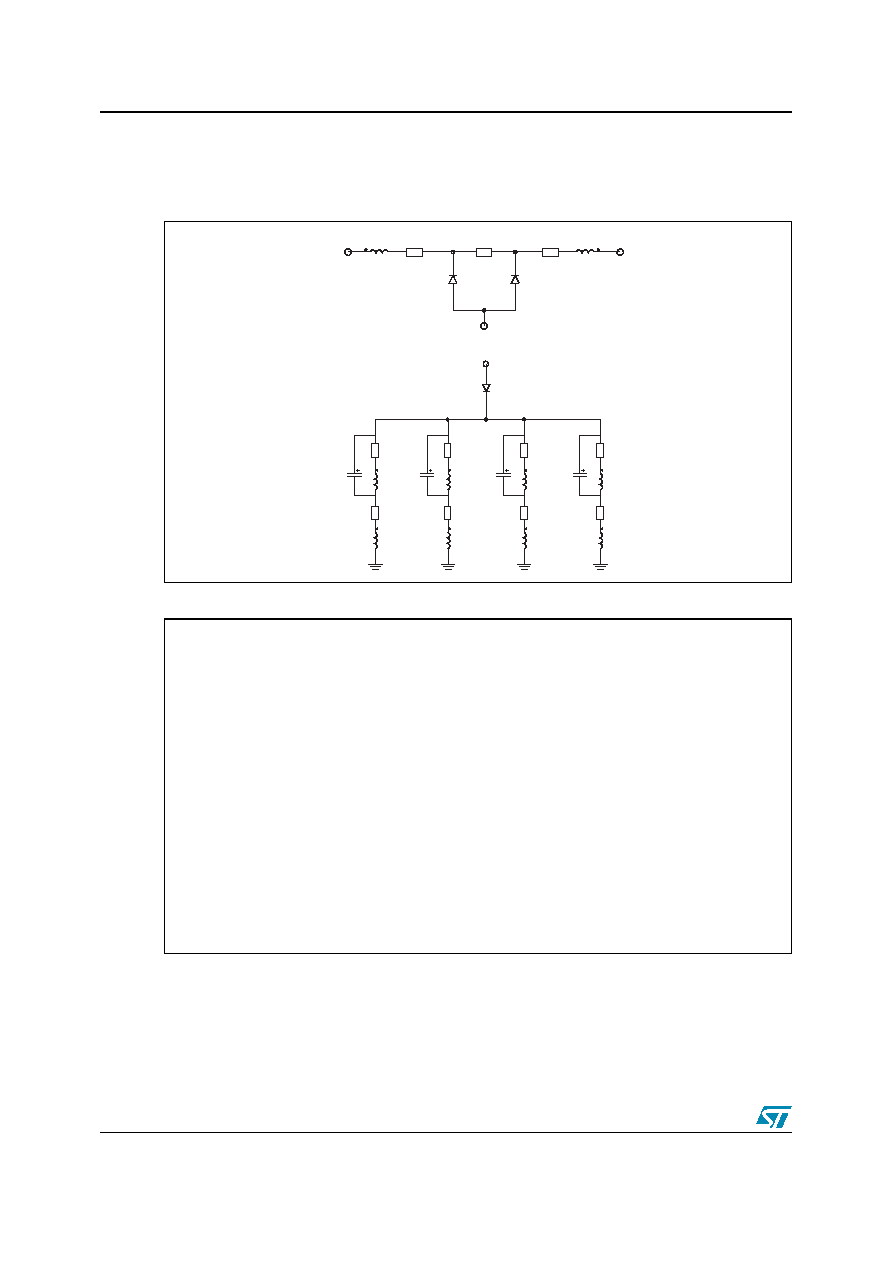
Pin Configuration (bump side)
Basic Cell Configuration
Complies with the following standards:
IEC61000-4-2:
on inputs and outputs
MIL STD 833E - Method 3015-6 Class 3
Part Number
Marking
EMIF07-LCD02F3
GX
Level 4
15 kV (air discharge)
8 kV ( contact discharge)
Flip-chip
(18 bumps)
A
B
C
D
1
2
3
4
5
O1
O2
O3
O4
O6
I5
O5
O7
I1
I2
I3
I7
I6
I4
GND
GND
GND
GND
Input
GND
GND
GND
Output
Low-pass Filter
Ri/o = 70
Cline = 30pF
www.st.com

1 Electrical characteristics (T
amb
= 25∞C)
EMIF07-LCD02F3
2/8
1
Electrical characteristics (T
amb
= 25∞C)
Table 1.
Absolute Maximum Ratings
Symbol
Parameter
Value
Unit
T
j
Junction temperature
125
∞C
T
op
Operating temperature range
-40 to + 85
∞C
T
stg
Storage temperature range
-55 to +150
∞C
Symbol
Parameter
V
BR
Breakdown voltage
I
RM
Leakage current @ V
RM
V
RM
Stand-off voltage
V
CL
Clamping voltage
I
PP
Peak pulse current
R
I/O
Series resistance between Input & Output
C
line
Input capacitance per line
Symbol
Test conditions
Min.
Typ.
Max.
Unit
V
BR
I
R
= 1 mA
6
8
10
V
I
RM
V
RM
= 3 V
50
200
nA
R
I/O
Tolerance ± 20 %
70
C
line
Vline = 0 V, V
OSC
= 30 mV, F =1 MHz
30
pF
I
V
I
F
I
RM
I
R
I
PP
V
RM
V
F
V
BR
V
CL

EMIF07-LCD02F3
1 Electrical characteristics (T
amb
= 25∞C)
3/8
Figure 1.
S21(dB) all lines attenuation
measurement and Aplac simulation
Figure 2.
Analog cross talk measurements
Figure 3.
Voltages when IEC61000-4-2 (+15kV
air discharge) applied to input pin
Figure 4.
Voltages when IEC61000-4-2 (-15kV
air discharge) applied to input pin
Figure 5.
Line capacitance versus applied
voltage
100.0k
1.0M
10.0M
100.0M
1.0G
-50.00
-40.00
-30.00
-20.00
-10.00
0.00
Line 1
Line 2
Line 3
Line 4
Line 5
Line 6
Line 7
100.0k
1.0M
10.0M
100.0M
1.0G
-100.00
-90.00
-80.00
-70.00
-60.00
-50.00
-40.00
-30.00
-20.00
-10.00
0.00
dB
f/Hz
Xtalk 1/2
100.0k
1.0M
10.0M
100.0M
1.0G
-100.00
-90.00
-80.00
-70.00
-60.00
-50.00
-40.00
-30.00
-20.00
-10.00
0.00
dB
f/Hz
Xtalk 1/2
100.0k
1.0M
10.0M
100.0M
1.0G
-100.00
-90.00
-80.00
-70.00
-60.00
-50.00
-40.00
-30.00
-20.00
-10.00
0.00
dB
f/Hz
Xtalk 1/2
Input
10V/d
Output
10V/d
100ns/d
Input
10V/d
Output
10V/d
100ns/d
0
5
10
15
20
25
30
0
1
2
3
4
5
6
V
(V)
line
C
(pF)
line

EMIF07-LCD02F3
3 Ordering information scheme
5/8
3 Ordering
information
scheme
EMIF yy - xxx zz F3
EMI Filter
Number of lines
Information
Package
x = resistance value (Ohms)
z = capacitance value / 10(pF)
or
3 letters = application
2 digits = version
F = Flip-Chip
3 = Lead free Pitch = 400µm, Bump = 255µm