
Æ
1/7
MAIN PRODUCT CHARACTERISTICS
EMI filtering and ESD protection for:
Computers and printers
Communication systems
Mobile phones
DESCRIPTION
The EMIF10-COM01F2 is a highly integrated
device designed to suppress EMI / RFI noise in all
systems subjected to electromagnetic interfer-
ences. The EMIF10 Flip-Chip packaging means
the package size is equal to the die size.
Additionally, this filter includes an ESD protection
circuitry which prevents the protected device from
destruction when subjected to ESD surges up to
15 kV.
BENEFITS
EMI symmetrical (I/O) low-pass filter
Lead free package
Very low PCB space consuming: < 6mm
2
Very thin package: 0.65 mm
High efficiency in ESD suppression on both
input & output pins
High reliability offered by monolithic integration
COMPLIES WITH THE FOLLOWING STANDARDS:
IEC61000-4-2 level 4
15kV (air discharge)
8kV (contact discharge)
EMIF10-COM01F2
EMI FILTER
INCLUDING ESD PROTECTION
REV. 2
April 2005
Flip-Chip
(25 Bumps)
Figure 1: Pin Configuration (Ball side)
1
2
3
4
5
E
D
C
B
A
02
04
03
05
06
09
08
010
07
GND
GND
GND
I1
I9
I8
I10
I2
I4
I3
GND
GND
I6
I7
01
I5
TM: IPAD is a trademark of STMicroelectronics.
Table 1: Order Code
Part Number
Marking
EMIF010-COM01F2
FE
Figure 2: Basic cell configuration
Output
Low-pass Filter
R
= 200
I/O
C
= 45 pF
line
Input
IPADTM
EMIF10-COM01F2
2/7
Table 2: Absolute Ratings (T
amb
= 25∞C)
Table 3: Electrical Characteristics (T
amb
= 25∞C)
Symbol
Parameter and test conditions
Value
Unit
V
PP
ESD discharge IEC61000-4-2, air discharge
ESD discharge IEC61000-4-2, contact discharge
15
8
kV
T
j
Junction temperature
125
∞C
T
op
Operating temperature range
- 40 to + 85
∞C
T
stg
Storage temperature range
- 55 to + 150
∞C
Symbol
Parameter
V
BR
Breakdown voltage
I
RM
Leakage current @ V
RM
V
RM
Stand-off voltage
V
CL
Clamping voltage
R
d
Dynamic impedance
I
PP
Peak pulse current
R
I/O
Series resistance between Input &
Output
C
line
Input capacitance per line
Symbol
Test conditions
Min.
Typ.
Max.
Unit
V
BR
I
R
= 1 mA
6 8 10 V
I
RM
V
RM
= 3V per line
500 nA
R
d
I
PP
= 10A, t
p
= 2.5µs
1
R
I/O
180 200 220
C
line
At 0V bias
45
50
pF
t
LH
Vinput = 2.8V Rload = 100k
25
ns
V
I
V
RM
PP
I
RM
I
V
BR
R
I
V
CL
slope : 1 / R
d

EMIF10-COM01F2
3/7
Figure 3: S21(db) attenuation measurement
Figure 4: Analog crosstalk
Note: Spikes at high frequencies are induced by the PCB layout
Figure 5: ESD response to IEC61000-4-2
(+15kV air discharge) on one input V(in) and on
one output (Vout)
Figure 6: ESD response to IEC61000-4-2 (-15kV
air discharge) on one input V(in) and on one
output (Vout)
Figure 7: Rise time measurement
1.0M
3.0M
10.0M
30.0M
100.0M
300.0M
1.0G
3.0G
-50.00
-45.00
-40.00
-35.00
-30.00
-25.00
-20.00
-15.00
-10.00
-5.00
0.00
EMIF10-COM01F2: Typical S21(dB) measurement on line I10/O10
dB
f/Hz
100.0k
1.0M
10.0M
100.0M
1.0G
-100.00
-90.00
-80.00
-70.00
-60.00
-50.00
-40.00
-30.00
-20.00
-10.00
0.00
dB
f/Hz
100.0k
1.0M
10.0M
100.0M
1.0G
-100.00
-90.00
-80.00
-70.00
-60.00
-50.00
-40.00
-30.00
-20.00
-10.00
0.00
dB
f/Hz
V(in1)
V(out1)
V(in1)
V(out1)
EMIF10-COM01F2
In
Out
Square signal
Generator Vc = 2.8V
100k
Vout
Vin
Vout
Vin
EMIF10-COM01F2
4/7
PCB grounding recommendations
In order to ensure a good efficiency in terms of ESD protection and filtering behavior, we recommend to
implement microvias (100 µm dia.) between the GND bumps and the GND layer. GND bumps can be con-
nected together in PCB layer 1, and in addition, if possible, use through hole vias (200
µm dia.) in both
sides of filter to improve contact to GND (layer). This layout will minimize the distance to the ground and
thus parasitic inductances. In addition, we recommend to have GND plane wherever possible.
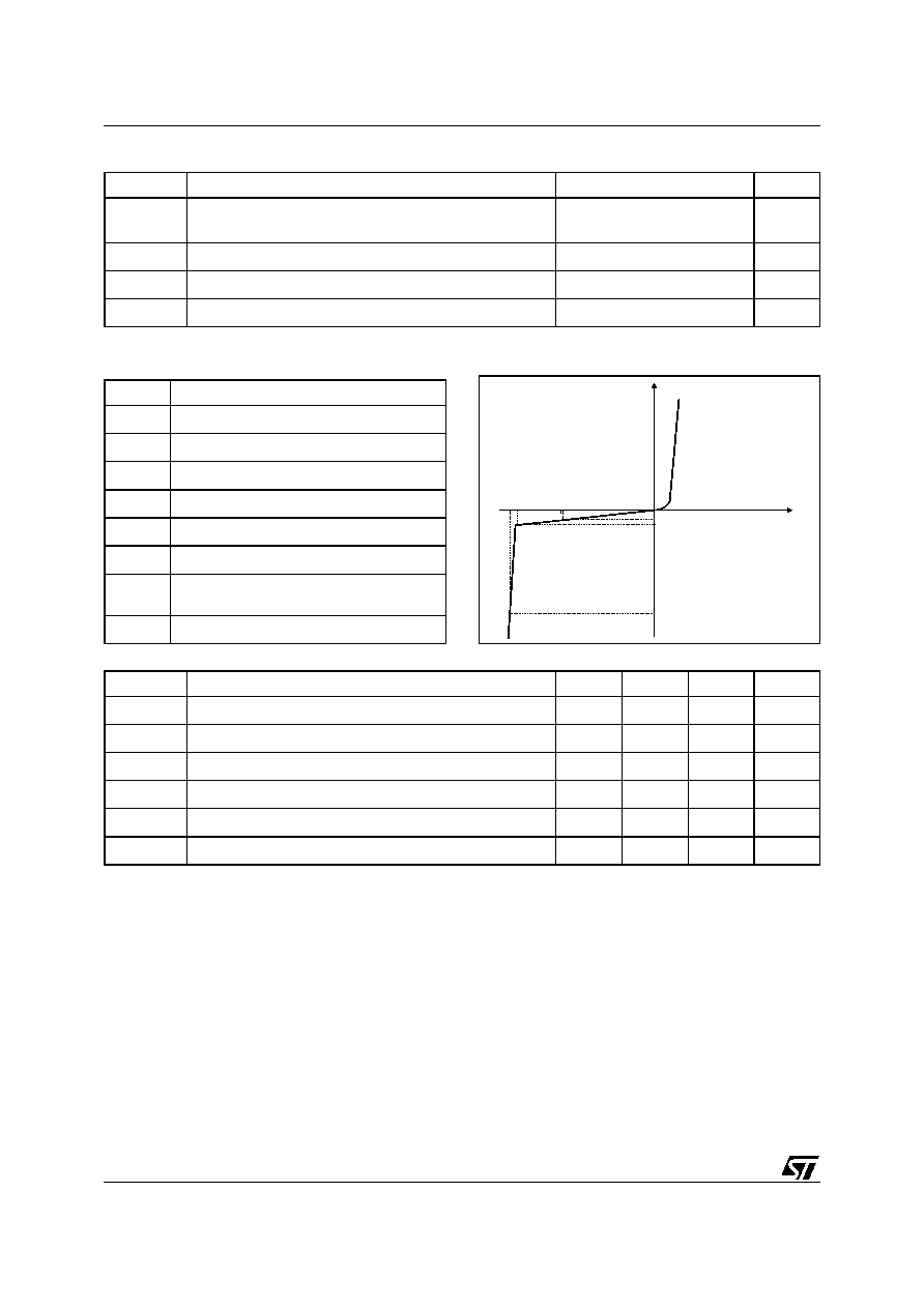
Figure 8: Capacitance versus reverse applied
voltage
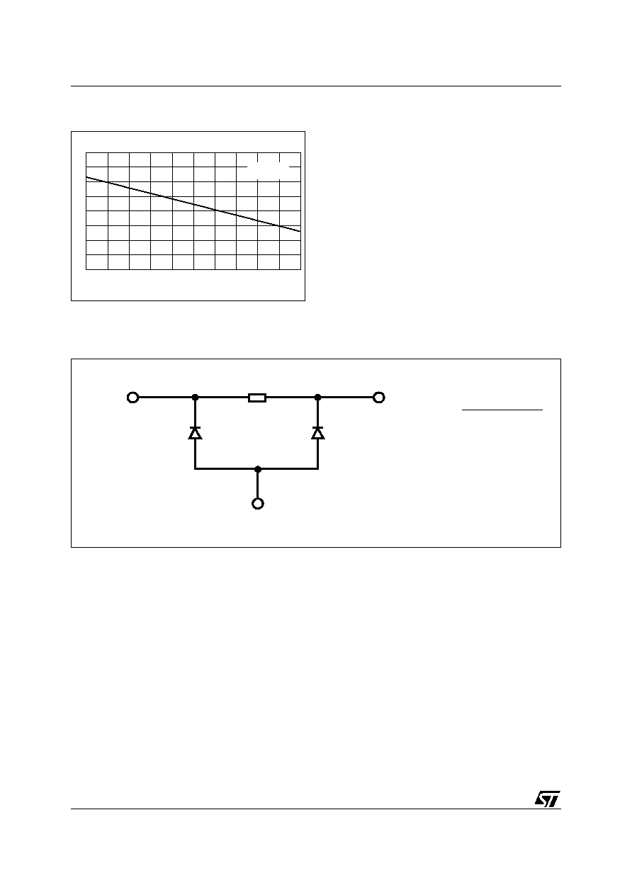
Figure 9: Aplac model
10
20
30
40
50
0
1
2
3
4
5
VR(V)
C(pF)
F=1MHz
Vosc=30mV
Demif10 model
BV = 7
IBV = 1m
CJO = 25p
M = 0.3333
RS = 1
VJ = 0.6
TT = 100n
out
in
200R
MODEL = demif10
MODEL = demif10
sub

EMIF10-COM01F2
5/7
Figure 10: Ordering Information Scheme
Figure 11: FLIP-CHIP Package Mechanical Data
Figure 12: Foot print recommendations
Figure 13: Marking
EMIF yy - xxx zz Fx
EMI Filter
Number of lines
Information
Package
x = resistance value (Ohms)
z = capacitance value / 10(pF)
or
3 letters = application
2 digits = version
F = Flip-Chip
x
= 1: 500µm, Bump = 315µm
= 2: Leadfree Pitch = 500µm, Bump = 315µm
= 3: Leadfree Pitch = 400µm, Bump = 250µm
2.42mm ± 50µm
2.42mm ± 50µm
315µm ± 50
500µm ± 50
500µm ± 50
650µm ± 65
Copper pad Diameter :
250µm recommended , 300µm max
Solder stencil opening : 330µm
Solder mask opening recommendation :
340µm min for 315µm copper pad diameter
545
545
400
100
230
x
y
x
w
z
w
All dimensions in µm
E
Dot, ST logo
xx = marking
yww = datecode
(y = year
ww = week)
z = packaging location