Rev 1
September 2005
1/8
8
ESDA14V2-4BF3
ASD (Application Specific Devices)
Quad bidirectional TRANSILTM array for ESD protection
Application
Where transient overvoltage protection in ESD
sensitive equipment is required, such as :
Computers
Printers
Communication systems and cellular phones
Video equipment
This device is particularly adapted to the
protection of symmetrical signals.
Description
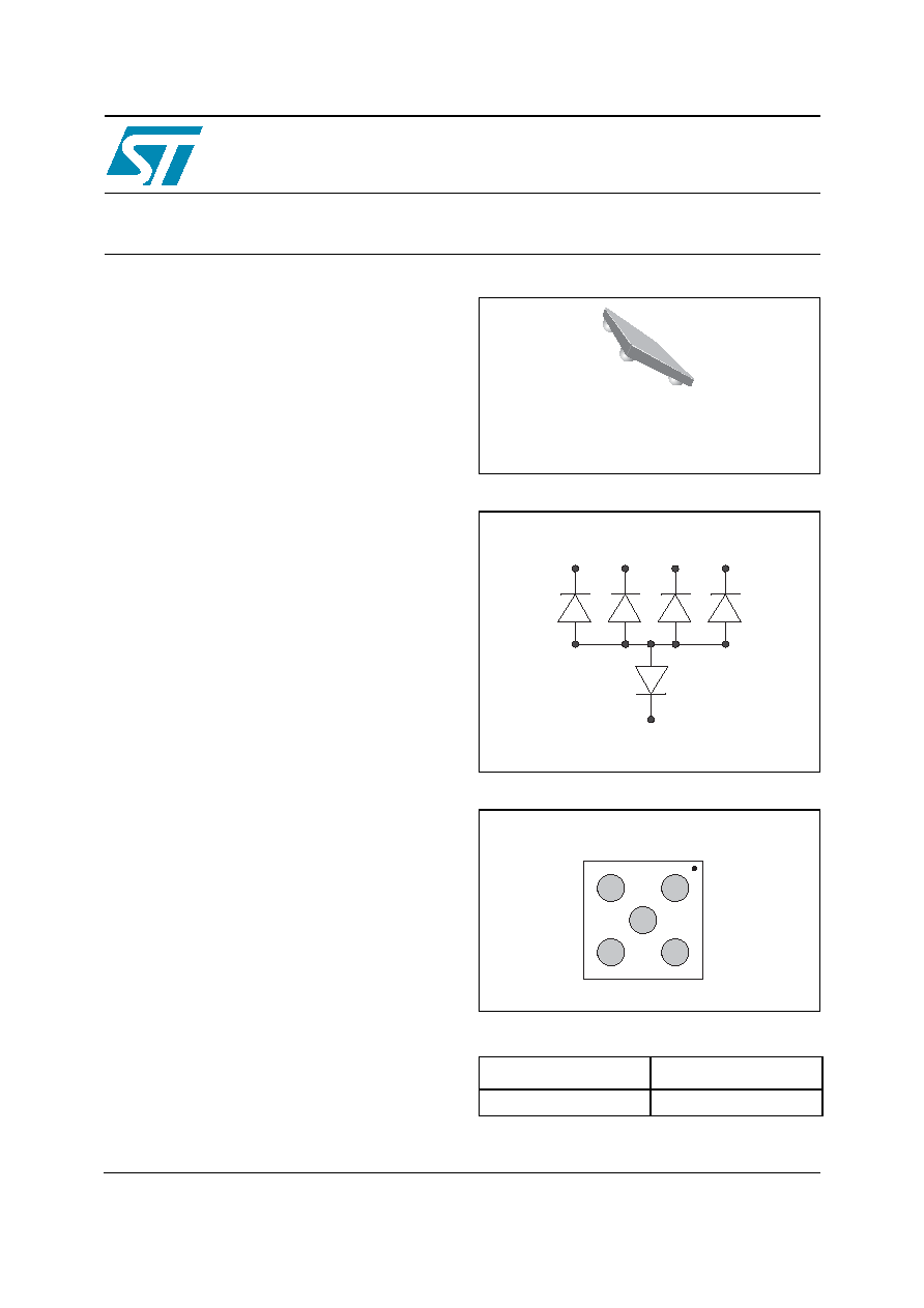
The ESDA14V2-4BF3 is a monolithic array
designed to protect up to 4 lines in a bidirectional
way against ESD transients.
The device is ideal for situations where board
space saving is requested.
Features
4 Bidirectional Transil functions
ESD Protection: IEC61000-4-2 level 4
Stand off voltage: 12 V Min.
Low leakage current < 0.5 µA
50 W Peak pulse power (8/20 µs)
Benefits
High ESD protection level
High integration
Suitable for high density boards
Complies with the following standards:
TM: TRANSIL is a trademark of STMicroelectronics
Configuration
Pin layout (bump side)
Order Code
IEC61000-4-2
15 kV
(air discharge)
8 kV
(contact discharge)
MIL STD 883E- Method 3015-7: class3
25 kV
(human body model)
Part number
Marking
ESDA14V2-4BF3
EF
Flip-Chip
(5 bumps)
GND
A1
A3
B2
C1
C3
A
B
C
3
1
2
www.st.com

1 Characteristics
ESDA14V2-4BF3
2/8
1 Characteristics
1.1
Absolute ratings (limiting values)
1.2
Electrical characteristics (T
amb
= 25 °C)
Symbol
Parameter
Value
Unit
V
PP
ESD discharge
MIL STD 883E - Method 3015-7
IEC61000-4-2 air discharge
IEC61000-4-2 contact discharge
± 25
± 15
± 8
kV
P
PP
Peak pulse power (8/20µs)
50
W
T
j
Junction temperature
125
°C
T
stg
Storage temperature range
-55 to +150
°C
T
L
Lead solder temperature (10 seconds duration)
260
°C
T
op
Operating temperature range
-40 to +125
°C
Symbol
Parameter
V
BR
Breakdown voltage
I
RM
Leakage current @ V
RM
V
RM
Stand-off voltage
V
CL
Clamping voltage
R
d
Dynamic impedance
I
PP
Peak pulse current
C
Capacitance
Part Number
V
BR
@ I
R
I
RM
@ V
RM
R
d
T
C
min.
max.
max.
typ.
(1)
1.
Square pulse, IPP = 3A, tp = 2.5µs.
max.
(2)
2.
VBR =
T (Tamb -25°C) x VBR (25°C)
max.
0V bias
V
V
mA
µA
V
10
-4
/°C
pF
ESDA14V2-4BF3
14.2
18
1
0.5
12
3.2
10
15
0.1
3
V
CL
V
BR
V
RM
I
PP
I
Slope: 1 / R
d
V

ESDA14V2-4BF3
1 Characteristics
3/8
Figure 1.
Clamping voltage versus peak
pulse current (T
j
initial = 25 °C)
(Rectangular waveform, t
p
= 2.5 µs)
Figure 2.
Junction capacitance versus
reverse applied voltage (typical
values)
Figure 3.
Relative variation of leakage
current versus junction
temperature (typical values)
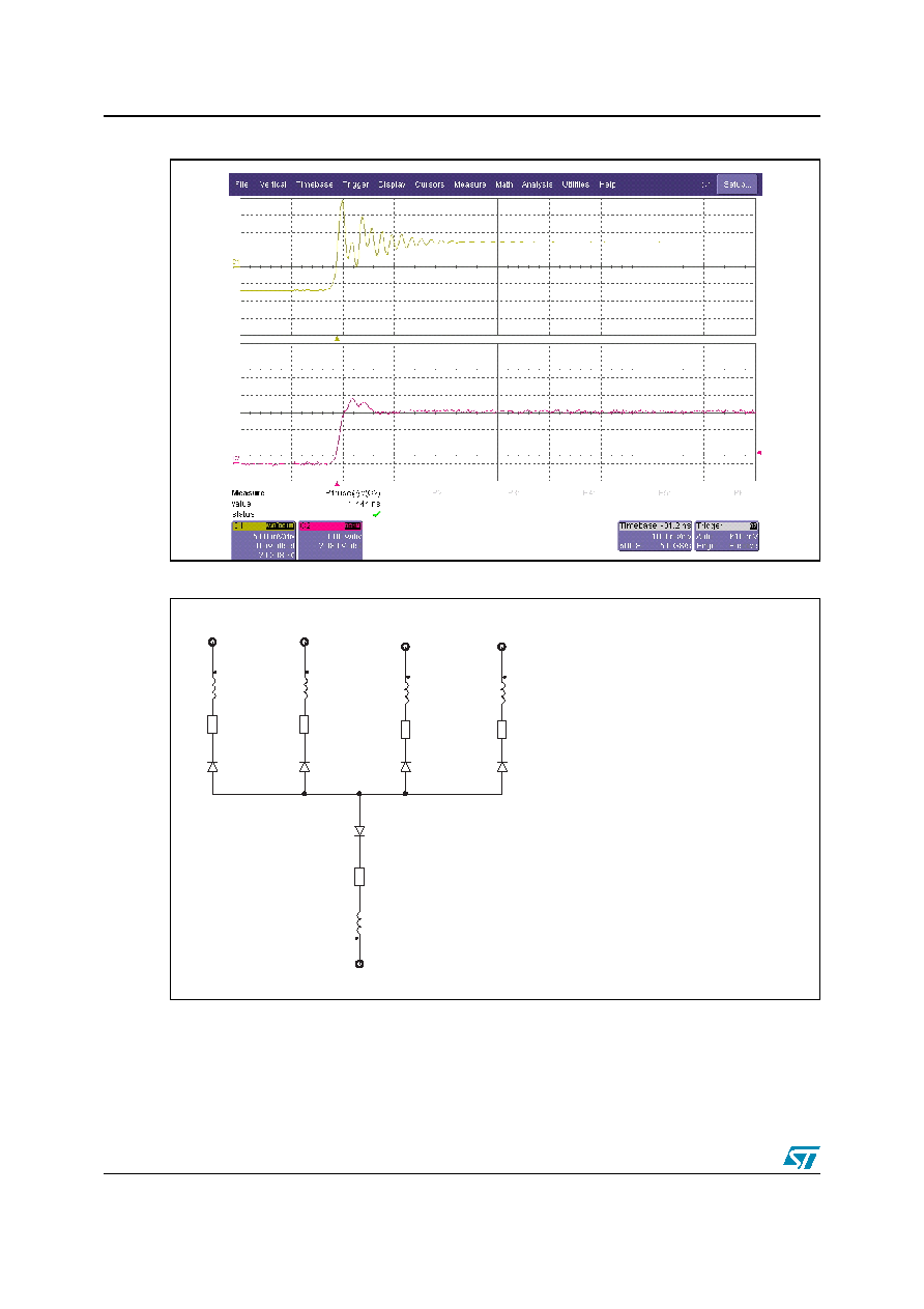
Figure 4.
ESD response to IEC61000-4-2
(+15 kV air discharge)
Figure 5.
ESD response to IEC61000-4-2
(-15 kV air discharge)
Figure 6.
Analog crosstalk measurements
0.1
1.0
10.0
0
10
20
30
40
50
60
I
PP
(A)
t
p
=2.5 µs
T
j
initial =25 °C
V
CL
(V)
0
2
4
6
8
10
12
14
16
0.0
0.5
1.0
1.5
2.0
2.5
3.0
3.5
4.0
4.5
5.0
C(pF)
F=1 MHz
V
OSC
=30 mV
RMS
T
j
=25 °C
V
R
(V)
1
10
100
25
50
75
100
125
I
R
[T
j
] / I
R
[T
j
=25 °C]
T
j
(°C)
100.0k
1.0M
10.0M
100.0M
1.0G
-120.00
-90.00
-60.00
-30.00
0.00
Xtalk
f/Hz
1 Characteristics
ESDA14V2-4BF3
4/8
Figure 7.
Digital crosstalk measurements
Figure 8.
Aplac model
MODEL = D01
Ls
MODEL = D01
MODEL = D01
MODEL = D01
Ls
Rs
Rs
Ls
Rs
MODEL = D02
Ls
A1
C3
A3
C1
B2
Rs
Lgnd
Rs
Model D01
BV=16
IBV=1m
CJO=12p
M=0.333
RS=2.9
VJ=0.6
TT=100n
Model D02
BV=16
IBV=1m
CJO=320p
M=0.333
RS=80m
VJ=0.6
TT=100n
aplacvar Ls 290pH
aplacvar Lgnd 130pH
aplacvar Rs 100m

ESDA14V2-4BF3
2 Ordering information scheme
5/8
2 Ordering
information
scheme
ESDA 14V2 - 4 B Fx
ESD Array
Number of line
Package
Breakdown Voltage
Type
14V2 = 14.2 Volts min.
B = Bidirectional
x = 3: Leadfree Pitch = 400µm, Bump height = 260µm
4 = 4 lines
F = Flip-Chip
x = 2: Leadfree Pitch = 500µm, Bump height = 315µm