1/5
ESDA14V2BP6
Æ
March 2003 - Ed: 3A
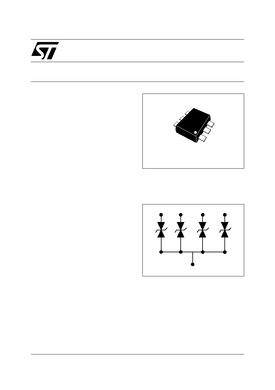
TRANSILTM
SOT-666
Where transient overvoltage protection in ESD
sensitive equipment is required, such as :
s
Computers
s
Printers
s
Communication systems and cellular phones
s
Video equipment
This device is particularly adpated to the protection
of symmetrical signals.
MAIN APPLICATIONS
Application Specific Discretes
A.S.D.TM
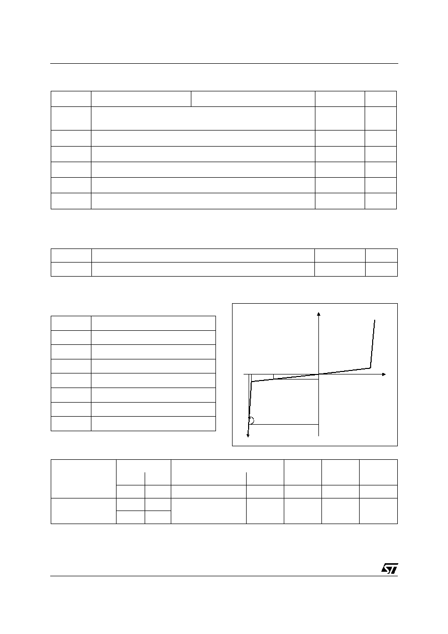
1
3
GND: 2, 5
6
4
FUNCTIONAL DIAGRAM
s
4 Bidirectional TransilTM functions.
s
ESD Protection: IEC61000-4-2 level 4
s
Stand off voltage: 12V MIN
s
Low leakage current < 1µA
FEATURES
The ESDA14V2BP6 is a monolithic array designed
to protect up to 4 lines in a bidirectional way against
ESD transients.
This device is ideal for applications where board
space saving is required.
DESCRIPTION
s
High ESD protection level.
s
High integration.
s
Suitable for high density boards.
BENEFITS
s
IEC61000-4-2 level 4: 15 kV (air discharge)
8 kV (contact discharge)
s
MIL STD 883E-Method 3015-7: class 3
25kV HBM (Human Body Model)
COMPLIES WITH THE FOLLOWING STANDARDS :
ESDA14V2BP6
2/5
Symbol
Parameter
V
RM
Stand-off voltage
V
BR
Breakdown voltage
V
CL
Clamping voltage
I
RM
Leakage current @ V
RM
I
PP
Peak pulse current
T
Voltage tempature coefficient
V
F
Forward voltage drop
ELECTRICAL CHARACTERISTICS (T
amb
= 25∞C)
V
I
V
CL
V
BR
V
RM
I
RM
I
PP
Slope: 1/R
d
Symbol
Parameter
Test conditions
Value
Unit
V
PP
ESD discharge - IEC61000-4-2 air discharge
IEC61000-4-2 contact discharge
± 15
± 8
kV
P
PP
Peak pulse power dissipation(8/20
µ
s). Note 1
T
j
initial = Tamb
50
W
T
j
Junction temperature
125
∞
C
T
stg
Storage temperature range
- 55 to + 150
∞C
T
L
Maximum lead temperature for soldering during 10s at 5mm for case
260
∞C
T
op
Operating temperature range
- 40 to + 125
∞C
Note 1: for a surge greater than the maximum values
,
the diode will fail in short-circuit.
ABSOLUTE RATINGS (T
amb
= 25∞C)
Types
I
RM
@ V
RM
V
BR
@
I
R
Rd
T
C
max.
min.
max.
typ.
typ.
max.
µA
V
V
V
mA
10
-4
/∞C
pF @ 0V
ESDA14V2BP6
1
12
14.2
18
1
1.5
5.8
25
0.1
3
Symbol
Parameter
Value
Unit
R
th(j-a)
Junction to ambient on printed circuit on recommended pad layout
220
∞C/W
THERMAL RESISTANCES
ESDA14V2BP6
3/5
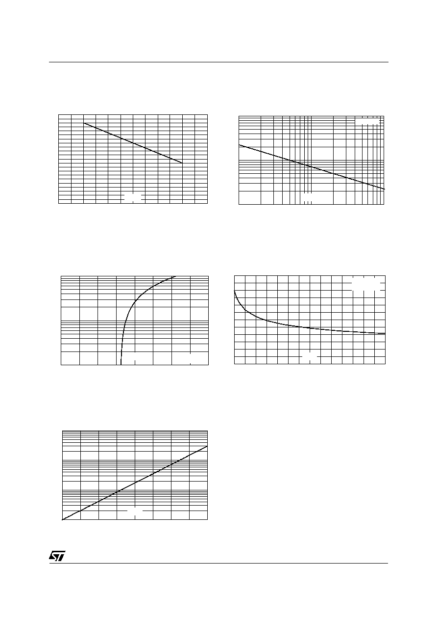
0.0
0.1
0.2
0.3
0.4
0.5
0.6
0.7
0.8
0.9
1.0
1.1
0
25
50
75
100
125
150
Tj (∞C)
P
[Tj initial] / P
[Tj initial = 25∞C]
PP
PP
Fig. 1: Relative variation of peak pulse power
versus initial junction temperature.
10
100
1000
1
10
100
t (µs)
P
T
j
initial = 25∞C
P
(W)
PP
Fig. 2: Peak pulse power versus exponential pulse
duration.
0.1
1.0
10.0
0
10
20
30
40
V
(V)
CL
t
P
=2.5µs
T
j
initial =25∞C
I
(A)
PP
Fig. 3: Clamping voltage versus peak pulse
current (typical values, rectangular waveform).
0
5
10
15
20
25
30
0
2
4
6
8
10
12
14
V (V)
R
F=1MHz
V
OSC
=30mV
RMS
T
j
=25∞C
C(pF)
Fig. 4: Junction capacitance versus reverse volt-
age applied (typical values).
1
10
100
1000
25
50
75
100
125
Tj(∞C)
IR[Tj] / IR[Tj = 25∞C]
Fig. 5: Relative variation of leakage current versus
junction temperature (typical values).
ESDA14V2BP6
4/5
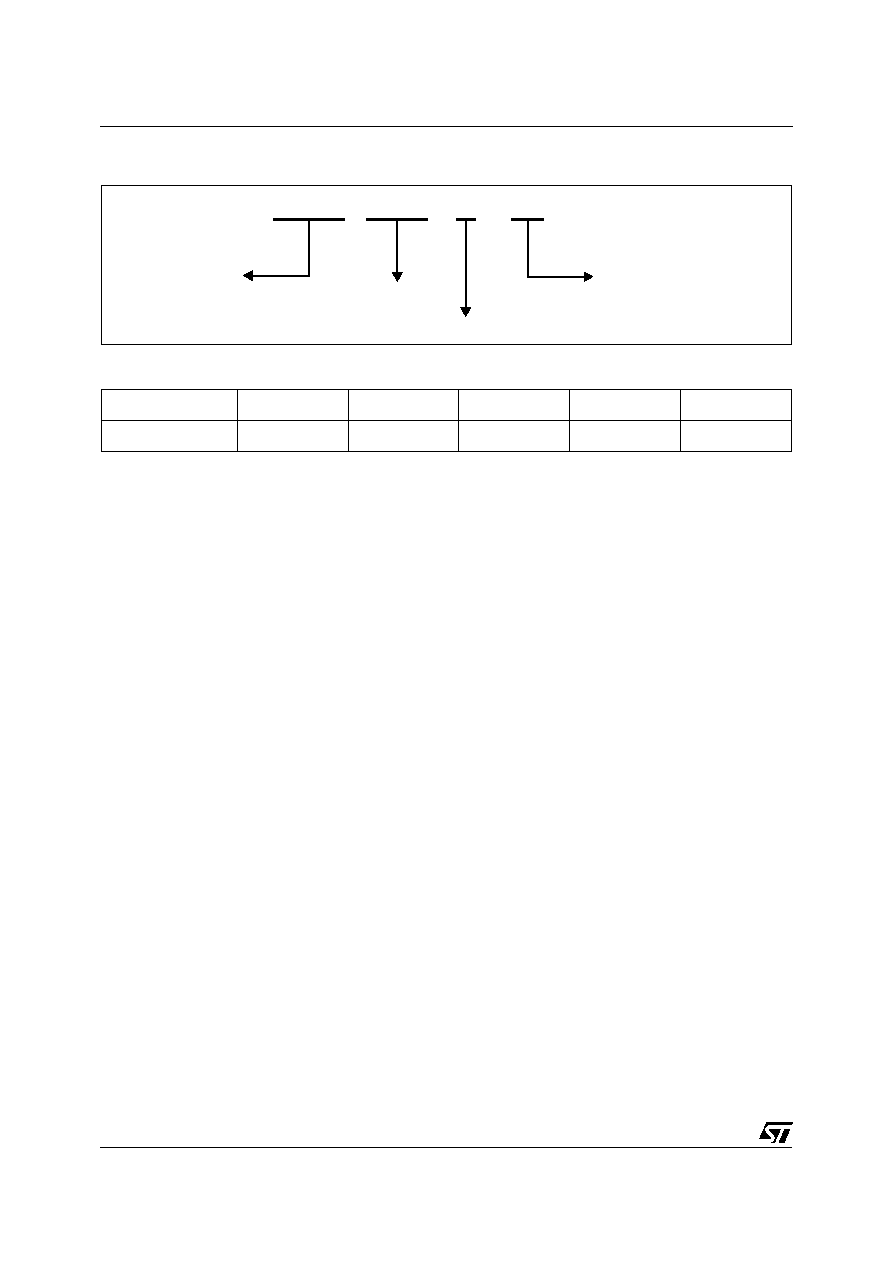
ESDA 14V2 B P6
ESD ARRAY
V
min
BR
PACKAGE: SOT-666
Bidirectional
ORDER CODE
Ordering type
Marking
Package
Weight
Base qty
Delivery mode
ESDA14V2BP6
A
SOT-666
2.9 mg.
3000
Tape & reel 7"

ESDA14V2BP6
5/5
PACKAGE MECHANICAL DATA
SOT-666
D
bp
e1
e
E
Lp
He
A
U
REF.
DIMENSIONS
Millimeters
Inches
Min.
Max.
Min.
Max.
A
0.50
0.60
0.020
0.024
bp
0.17
0.27
0.007
0.011
c
0.08
0.18
0.003
0.007
D
1.50
1.70
0.060
0.067
E
1.10
1.30
0.043
0.051
e
1.00
0.040
e1
0.50
0.020
He
1.50
1.70
0.059
0.067
Lp
0.10
0.30
0.004
0.012
0.36
0.30
0.84
0.20
0.20
0.62
2.30
FOOT PRINT (in millimeters)
Information furnished is believed to be accurate and reliable. However, STMicroelectronics assumes no responsibility for the consequences of
use of such information nor for any infringement of patents or other rights of third parties which may result from its use. No license is granted by
implication or otherwise under any patent or patent rights of STMicroelectronics. Specifications mentioned in this publication are subject to
change without notice. This publication supersedes and replaces all information previously supplied.
STMicroelectronics products are not authorized for use as critical components in life support devices or systems without express written ap-
proval of STMicroelectronics.
The ST logo is a registered trademark of STMicroelectronics
© 2003 STMicroelectronics - Printed in Italy - All rights reserved.
STMicroelectronics GROUP OF COMPANIES
Australia - Brazil - Canada - China - Finland - France - Germany
Hong Kong - India - Israel - Italy - Japan - Malaysia - Malta - Morocco - Singapore
Spain - Sweden - Switzerland - United Kingdom - United States.
http://www.st.com