 | –≠–ª–µ–∫—Ç—Ä–æ–Ω–Ω—ã–π –∫–æ–º–ø–æ–Ω–µ–Ω—Ç: ESDA17SC6 | –°–∫–∞—á–∞—Ç—å:  PDF PDF  ZIP ZIP |

1/9
ESDAxxSC5
ESDAxxSC6
QUAD TRANSIL ARRAY
FOR ESD PROTECTION
Æ
SOT23-5L (SC-59)
ESDAxxSC5
The ESDAxxSC5 and ESDAxxSC6 are monolithic
voltage
suppressors
designed
to
protect
components which are connected to data and
transmission lines against ESD.
They clamp the voltage just above the logic level
supply for positive transients, and to a diode drop
below ground for negative transient.
DESCRIPTION
May 2002 Ed: 6F
Where transient overvoltage protection in ESD
sensitive equipment is required, such as :
- Computers
- Printers
- Communication systems
- Cellular phone handsets and accessories
- Other telephone set
- Set top boxes
APPLICATIONS
SOT23-6L (SC-59)
ESDAxxSC6
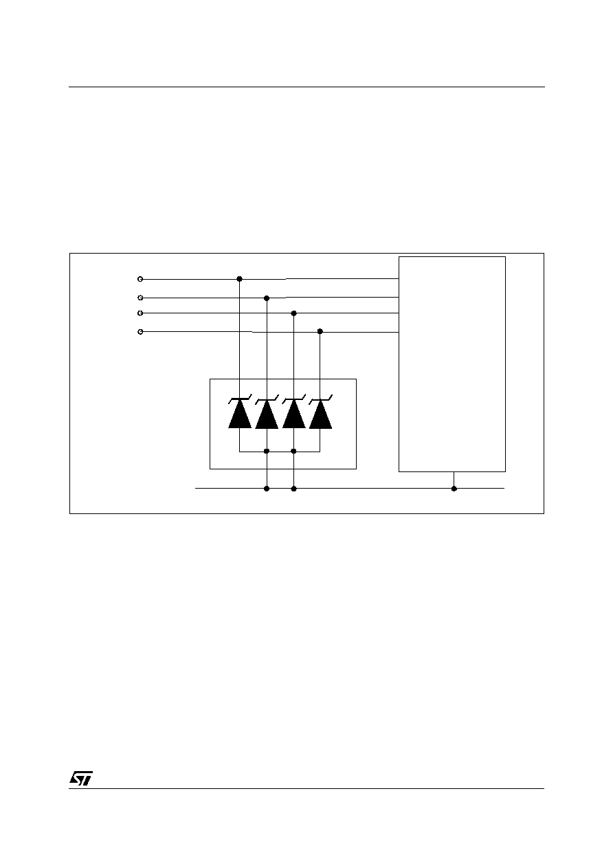
FUNCTIONAL DIAGRAM
SOT23-5L
SOT23-6L
Application Specific Di
scretes
A.S.D.TM
High ESD protection level : up to 25 kV
High integration
Suitable for high density boards
BENEFITS
IEC61000-4-2 : level 4
15kV (air discharge)
8kV (contact discharge)
MIL STD 883E-Method 3015-7 : class3B
(human body model)
COMPLIES
WITH
THE
FOLLOWING
STAN-
DARDS:
s
4 Unidirectional TransilTM Functions
s
Low leakage current: I
R
max. < 20
µ
A at V
BR
s
500 W Peak pulse power (8/20
µ
s)
FEATURES
1
2
3
5
4
1
2
3
6
5
4

ESDAxxSC5 / ESDAxxSC6
2/9
Symbol
Test conditions
Value
Unit
V
PP
ESD discharge - MIL STD 883E - Method 3015-7
IEC61000-4-2 air discharge
IEC61000-4-2 contact discharge
25
kV
P
PP
Peak pulse power (8/20
µ
s) note1
ESDA5V3SCx
ESDA6V1SCx
500
W
ESDA14V2SCx
ESDA17SC6
ESDA19SC6
ESDA25SC6
300
W
T
j
Junction temperature
150
∞C
T
stg
Storage temperature range
-55 to +150
∞C
T
L
Lead solder temperature (10 second duration)
260
∞
C
T
op
Operating temperature range
-40 to +125
∞
C
ABSOLUTE MAXIMUM RATINGS (T
amb
= 25∞C)
I
IF
V F
VBR
VRM
I PP
I RM
V
Rd
V
CL
Symbol
Parameter
V
RM
Stand-off voltage
V
BR
Breakdown voltage
V
CL
Clamping voltage
I
RM
Leakage current
I
PP
Peak pulse current
T
Voltage temperature coefficient
C
Capacitance
Rd
Dynamic resistance
V
F
Forward voltage drop
ELECTRICAL CHARACTERISTICS (T
amb
= 25∞C)

ESDAxxSC5 / ESDAxxSC6
3/9
The ESDA family has been designed to clamp fast
spikes like ESD. Generally the PCB designers
need to calculate easily the clamping voltage V
CL
.
This is why we give the dynamic resistance in
addition to the classical parameters. The voltage
across the protection cell can be calculated with
the following formula:
V
CL
= V
BR
+ Rd I
PP
Where Ipp is the peak current through the ESDA cell.
DYNAMIC RESISTANCE MEASUREMENT
The short duration of the ESD has led us to prefer
a more adapted test wave, as below defined, to the
classical 8/20
µ
s and 10/1000
µ
s surges.
2.5 s duration measurement wave.
As the value of the dynamic resistance remains
stable for a surge duration lower than 20
µ
s, the
2.5
µ
s rectangular surge is well adapted. In
addition both rise and fall times are optimized to
avoid any parasitic phenomenon during the
measurement of Rd.
CALCULATION OF THE CLAMPING VOLTAGE
USE OF THE DYNAMIC RESISTANCE
2µs
tp = 2.5µs
t
I
Ipp
Types
V
BR
@
I
R
I
RM
@ V
RM
Rd
T
C
V
F
@
I
F
min.
max.
max.
typ.
max.
typ.
max.
note 1
note 2
0V bias
V
V
mA
µ
A
V
m
10
-4
/∞C
pF
V
mA
ESDA5V3SC5
ESDA5V3SC6
5.3
5.9
1
2
3
230
5
280
1.25
200
ESDA6V1SC5
ESDA6V1SC6
6.1
7.2
1
20
5.25
350
6
190
1.25
200
ESDA14V2SC5
ESDA14V2SC6
14.2
15.8
1
5
12
650
10
100
1.25
200
ESDA17SC6
ESDA19SC6
17
19
19
21
1
1
0.075
0.1
14
15
700
800
10
8.5
85
80
1.2
1.2
10
10
ESDA25SC6
25
30
1
1
24
1000
10
60
1.2
10
note 1 : Square pulse, Ipp = 15A, tp=2.5
µ
s.
note 2 :
VBR =
T* (Tamb -25∞C) * VBR (25∞C)

ESDAxxSC5 / ESDAxxSC6
4/9
0
25
50
75
100
125
150
0.0
0.1
0.2
0.3
0.4
0.5
0.6
0.7
0.8
0.9
1.0
1.1
Tj initial(∞C)
Ppp [Tj initial] / Ppp [Tj initial=25∞C]
Fig. 1: Peak power dissipation versus initial
junction temperature.
1
10
100
100
1000
5000
tp(µs)
Ppp(W)
ESDA14V2SC5/SC6
ESDA17SC6
ESDA19SC6
ESDA25SC6
ESDA5V3SC5/SC6
&
ESDA6V1SC5/SC6
Fig. 2: Peak pulse power versus exponential pulse
duration (Tj initial = 25 ∞C).
0
5 10 15 20 25 30 35 40 45 50 55 60 65 70 75 80
0.1
1.0
10.0
50.0
Vcl(V)
Ipp(A)
tp=2.5µs
ESDA5V3SC5/SC6
ESDA6V1SC5/SC6
ESDA14V2SC5/SC6
ESDA25SC6
ESDA17SC6
ESDA19SC6
Fig. 3: Clamping voltage versus peak pulse
current (Tj initial = 25 ∞C).
Rectangular waveform (tp = 2.5
µ
s).
1
2
5
10
20
50
10
100
500
VR(V)
C(pF)
F=1MHz
Vosc=30mV
ESDA6V1SC5/SC6
ESDA14V2SC5/SC6
ESDA5V3SC5/SC6
ESDA25SC6
ESDA19SC6
ESDA17SC6
Fig. 4: Capacitance versus reverse applied
voltage (typical values).
25
50
75
100
125
1
10
100
500
Tj(∞C)
IR[Tj] / IR[Tj=25∞C]
ESDA14V2SC5/SC6
&
ESDA6V1SC5/SC6
ESDA5V3SC5/SC6
ESDA25SC6
ESDA17SC6
&
ESDA19SC6
Fig. 5: Relative variation of leakage current versus
junction temperature (typical values).
0.5
1.0
1.5
2.0
2.5
3.0
3.5
4.0
0.01
0.10
1.00
5.00
VFM(V)
IFM(A)
ESDA25SC6
ESDA17SC6
ESDA5V3SC5/SC6
ESDA14V2SC5/SC6
&
ESDA6V1SC5/SC6
ESDA19SC6
Fig. 6: Peak forward voltage drop versus peak
forward current (typical values).
ESDAxxSC5 / ESDAxxSC6
5/9
Electrostatic discharge (ESD) is a major cause of
failure in electronic systems.
Transient Voltage Suppressors (TVS) are an ideal
choice for ESD protection. They are capable of
clamping the incoming transient overvoltage to a
low enough level such that damage to the
protected semiconductor is prevented.
Surface mount TVS arrays offer the best choice for
minimal lead inductance.
They serve as parallel protection elements,
connected between the signal line and ground. As
the transient rises above the operating voltage of
the device, the TVS array becomes a low
impedance path diverting the transient current to
ground.
ESD protection by ESDAXXXSCX
ESD
sensitive
device
GND
ESDAxxxSC6
(1connection to GND for ESDAxxSC5)
I/ O LINES
The ESDAxxSCx array is the ideal board level
protection
of
ESD
sensitive
semiconductor
components.
The tiny SOT23-5L and SOT23-6L packages allow
design flexibility in the high density boards where
the space saving is at a premium. This enables to
shorten the routing and contributes to hardening
against ESD.
ADVICE FOR OPTIMIZING CIRCUIT BOARD
LAYOUT
Circuit board layout is a critical design step in the
suppression of ESD induced transients. The
following guidelines are recommended :
s
The ESDAxxSC5/6 should be placed as close as
possible to the input terminals or connectors.
s
The path length between the ESD suppressor
and the protected line should be minimized
s
All conductive loops, including power and
ground loops should be minimized
s
The ESD transient return path to ground should
be kept as short as possible.
s
Ground planes should be used whenever possi-
ble.