
STE53NA50
N - CHANNEL ENHANCEMENT MODE
FAST POWER MOS TRANSISTOR
s
TYPICAL R
DS(on)
= 0.075
s
HIGH CURRENT POWER MODULE
s
AVALANCHE RUGGED TECHNOLOGY
s
VERY LARGE SOA - LARGE PEAK POWER
CAPABILITY
s
EASY TO MOUNT
s
SAME CURRENT CAPABILITY FOR THE
TWO SOURCE TERMINALS
s
EXTREMELY LOW Rth (Junction to case)
s
VERY LOW INTERNAL PARASITIC
INDUCTANCE
s
ISOLATED PACKAGE UL RECOGNIZED
APPLICATIONS
s
SMPS & UPS
s
MOTOR CONTROL
s
WELDING EQUIPMENT
s
OUTPUT STAGE FOR PWM, ULTRASONIC
CIRCUITS
INTERNAL SCHEMATIC DIAGRAM
February 1998
ABSOLUTE MAXIMUM RATINGS
Symbol
Parameter
Value
Uni t
V
DS
Drain-source Voltage (V
G S
= 0)
500
V
V
DGR
Drain- gate Voltage (R
G S
= 20 k
)
500
V
V
GS
Gate-source Voltage
±
30
V
I
D
Drain Current (continuous) at T
c
= 25
o
C
53
A
I
D
Drain Current (continuous) at T
c
= 100
o
C
33
A
I
DM
(
∑
)
Drain Current (pulsed)
212
A
P
to t
Total Dissipation at T
c
= 25
o
C
460
W
Derat ing Fact or
3.68
W/
o
C
T
st g
St orage Temperature
-55 to 150
o
C
T
j
Max. Operating Junction T emperat ure
150
o
C
V
ISO
Insulation W ithhstand Voltage (AC-RMS)
2500
V
(
∑
) Pulse width limited by safe operating area
TYPE
V
DSS
R
DS(on)
I
D
ST E53NA50
500 V
< 0.085
53 A
ISOTOP
1/7
THERMAL DATA
R
t hj-ca se
R
thc -h
Thermal Resistance Junction-case
Max
Thermal Resistance Case-heatsink W ith Conductive
Grease Applied
Max
0.27
0.05
o
C/W
o
C/W
AVALANCHE CHARACTERISTICS
Symb ol
Parameter
Max Valu e
Uni t
I
AR
Avalanche Current, Repetitive or Not -Repet itive
(pulse width limited by T
j
max,
< 1%)
26
A
E
AS
Single Pulse Avalanche Energy
(starting T
j
= 25
o
C, I
D
= I
AR
, V
DD
= 50 V)
1014
mJ
ELECTRICAL CHARACTERISTICS (T
case
= 25
o
C unless otherwise specified)
OFF
Symb ol
Parameter
Test Cond ition s
Mi n.
Typ .
Max.
Un it
V
(BR)DSS
Drain-source
Breakdown Volt age
I
D
= 1 mA
V
GS
= 0
500
V
I
DSS
Zero G ate Voltage
Drain Current (V
GS
= 0)
V
DS
= Max Rating
V
DS
= Max Rating
T
c
= 125
o
C
100
1000
µ
A
µ
A
I
GSS
Gate-body Leakage
Current (V
DS
= 0)
V
G S
=
±
30 V
±
400
nA
ON (
)
Symb ol
Parameter
Test Cond ition s
Mi n.
Typ .
Max.
Un it
V
GS(th)
Gate Threshold
Voltage
V
DS
= V
GS
I
D
= 1 mA
2.25
3
3.75
V
R
DS( on)
St atic Drain-source On
Resistance
V
G S
= 10V
I
D
= 27 A
0.075
0.085
I
D(o n)
On St ate Drain Current
V
DS
> I
D(on)
x R
DS(on) max
V
G S
= 10 V
53
A
DYNAMIC
Symb ol
Parameter
Test Cond ition s
Mi n.
Typ .
Max.
Un it
g
fs
(
)
Forward
Transconduct ance
V
DS
>I
D(on )
X
RDS(on)MAX
I
D
= 27 A
25
S
C
iss
C
oss
C
rss
Input Capacitance
Output Capacit ance
Reverse T ransfer
Capacitance
V
DS
= 25 V
f = 1 MHz
V
GS
= 0
13
1500
450
16
2000
650
nF
pF
pF
STE53NA50
2/7
ELECTRICAL CHARACTERISTICS (continued)
SWITCHING ON
Symb ol
Parameter
Test Cond ition s
Mi n.
Typ .
Max.
Un it
t
d(on)
t
r
Turn-on Time
Rise Time
V
DD
= 250 V
I
D
= 27 A
R
G
= 4.7
V
G S
= 10 V
(see test circuit, figure 1)
57
92
80
130
ns
ns
Q
g
Q
gs
Q
gd
Total Gate Charge
Gate-Source Charge
Gate-Drain Charge
V
DD
= 400 V
I
D
= 53 A V
G S
= 10 V
470
54
219
658
nC
nC
nC
SWITCHING OFF
Symb ol
Parameter
Test Cond ition s
Mi n.
Typ .
Max.
Un it
t
r(Vof f)
t
f
t
c
Of f-voltage Rise Time
Fall Time
Cross-over Time
V
DD
= 400 V
I
D
= 53 A
R
G
= 4.7
V
GS
= 10 V
(see test circuit, figure 3)
105
36
145
145
50
205
ns
ns
ns
SOURCE DRAIN DIODE
Symb ol
Parameter
Test Cond ition s
Mi n.
Typ .
Max.
Un it
I
SD
I
SDM
(
∑
)
Source-drain Current
Source-drain Current
(pulsed)
53
212
A
A
V
SD
(
)
Forward On Voltage
I
SD
= 53 A
V
GS
= 0
1.6
V
t
rr
Q
rr
I
RRM
Reverse Recovery
Time
Reverse Recovery
Charge
Reverse Recovery
Current
I
SD
= 53 A
di/dt = 100 A/
µ
s
V
R
= 100 V
T
j
= 150
o
C
(see test circuit, figure 3)
1000
31. 5
63
ns
µ
C
A
(
) Pulsed: Pulse duration = 300
µ
s, duty cycle 1.5 %
(
∑
) Pulse width limited by safe operating area
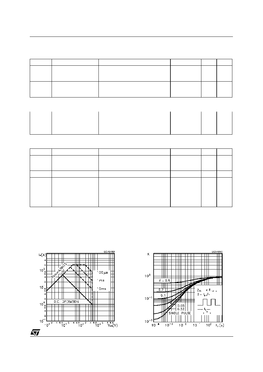
Safe Operating Area for
Thermal Impedance
STE53NA50
3/7
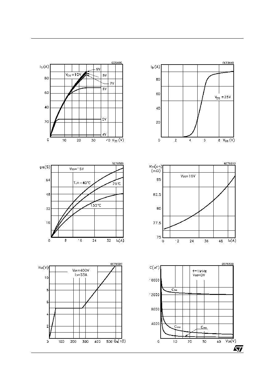
Output Characteristics
Transconductance
Gate Charge vs Gate-source Voltage
Transfer Characteristics
Static Drain-source On Resistance
Capacitance Variations
STE53NA50
4/7
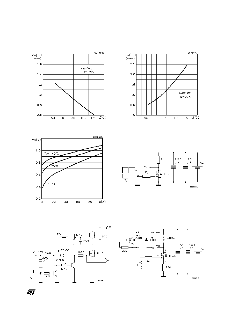
Normalized Gate Threshold Voltage vs
Temperature
Source-drain Diode Forward Characteristics
Fig. 2: Gate Charge test Circuit
Normalized On Resistance vs Temperature
Fig. 1: Switching Times Test Circuits For
Resistive Load
Fig. 3: Test Circuit For Inductive Load Switching
And Diode Recovery Times
STE53NA50
5/7