 | ÐлекÑÑоннÑй компоненÑ: ESDA25W5 | СкаÑаÑÑ:  PDF PDF  ZIP ZIP |
QUAL TRANSIL ARRAY FOR ESD PROTECTION

1/5
ESDA25W5
®
March 2000 - Ed: 1A
QUAL TRANSIL
TM
ARRAY
FOR ESD PROTECTION
SOT323-5L
Where transient overvoltage protection in ESD
sensitive equipment is required, such as :
n
Computers
n
Printers
n
Communication systems
n
Cellular phones handsets and accessories
n
Other telephone sets
n
Set top boxes
MAIN APPLICATIONS
Application Specific Discretes
A.S.D.
TM
FUNCTIONAL DIAGRAM
1
2
3
4
5
n
4 unidirectional TRANSIL
TM
functions.
n
150W peak pulse power (8/20
µ
s)
n
Breakdown voltage : V
BR
= 25V min.
n
Low leakage current : < 1
µ
A.
n
Very low PCB space consuming : 4.2 mm
2
typically.
FEATURES
DESCRIPTION
The ESDA25W5 is a 4-bit wide monolithic
suppressor designed to protect components
which are connected to data and transmission
lines against ESD.
It clamps the voltage just above the logic level
supply for positive transients, and to a diode drop
below ground for negative transients.
BENEFITS
n
High ESD protection level : up to 25 kV.
n
High integration.
n
Suitable for high density boards.
n
IEC61000-4-2 level 4
n
MIL STD 883C-Method 3015-6 : class 3.
(human body model)
COMPLIES WITH THE FOLLOWING STANDARDS :
ESDA25W5
2/5
Symbol
Parameter
V
RM
Stand-off voltage
V
BR
Breakdown voltage
V
CL
Clamping voltage
I
RM
Leakage current
I
PP
Peak pulse current
T
Voltage temperature coefficient
C
Capacitance per line
Rd
Dynamic resistance
V
F
Forward voltage drop
ELECTRICAL CHARACTERISTICS (T
amb
= 25°C)
V
I
V
RM
PP
I
RM
I
V
BR
R
I
V
CL
slope : 1 / R
d
Symbol
Parameter
Test conditions
Value
Unit
V
PP
ESD discharge
MIL STD 883C - Method 3015-6
IEC61000-4-2, air discharge
IEC61000-4-2, contact discharge
25
16
9
kV
P
PP
Peak pulse power (8/20
µ
s)
150
W
T
op
Operating temperature range
Note 1
- 40 to + 85
°C
T
j
Junction temperature
150
°C
T
stg
Storage temperature range
- 55 to + 150
°C
T
L
Lead solder temperature (10 secondes duration)
260
°C
Note 1: The evolution of the operating parameters versus temperature is given trough curves and
T parameter
ABSOLUTE MAXIMUM RATINGS (T
amb
= 25°C)
Types
V
BR
@
I
R
I
RM
@
V
RM
Rd
T
C
V
F
@
I
F
min.
max.
max.
typ.
max.
typ.
max.
note 2
note 3
0V bias
V
V
mA
µ
A
V
10
-4
/ °C
pF
V
mA
ESDA25W5
25
30
1
1
24
1.9
10
30
1.2
10
note 2 : Square pulse Ipp = 15A, tp=2.5
µ
s.
note 3 :
VBR =
T* (Tamb -25°C) * VBR (25°C)

ESDA25W5
3/5
25
50
75
100
125
150
1
10
100
Tj(°C)
IR[Tj] / IR[Tj=25°C]
Fig. 5: Relative variation of leakage current versus
junction temperature (typical values).
0.0
0.5
1.0
1.5
2.0
2.5
3.0
3.5
4.0
1E-8
3E-8
1E-7
3E-7
1E-6
3E-6
1E-5
3E-5
1E-4
VFM(V)
IFM(A)
Tj=25°C
Fig. 6: Peak forward voltage drop versus peak
forward current (typical values).
25
30
35
40
45
50
55
60
65
70
0.1
1.0
10.0
100.0
Vcl(V)
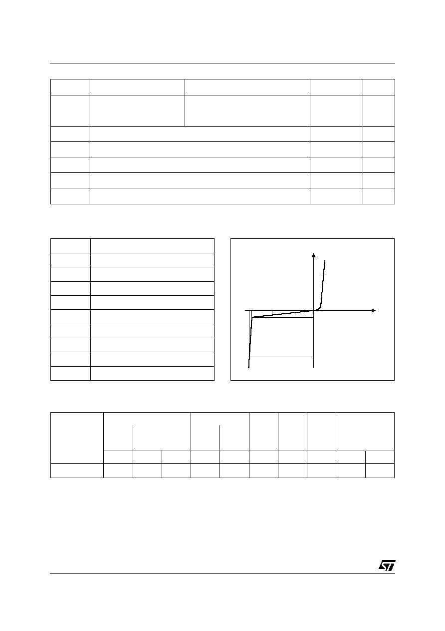
Ipp(A)
tp=2.5µs
Fig.
3: Clamping voltage versus peak pulse
current (Tj initial = 25 °C).
Rectangular waveform tp = 2.5
µ
s.
1
1
10
10
100
100
VR(V)
C(pF)
F=1MHz
Vosc=30mV
Fig. 4: Capacitance versus reverse applied
voltage (typical values).
0
25
50
75
100
125
150
0.0
0.1
0.2
0.3
0.4
0.5
0.6
0.7
0.8
0.9
1.0
1.1
Ppp [Tj initial] / Ppp [Tj initial=25°C]
Tj initial (°C)
Fig. 1: Peak pulse power dissipation versus initial
junction temperature
1000
1
10
10
100
100
tp(µs)
Ppp(W)
Fig.
2: Peak pulse power versus exponential
pulse duration (Tj initial = 25 °C)
ESDA25W5
4/5
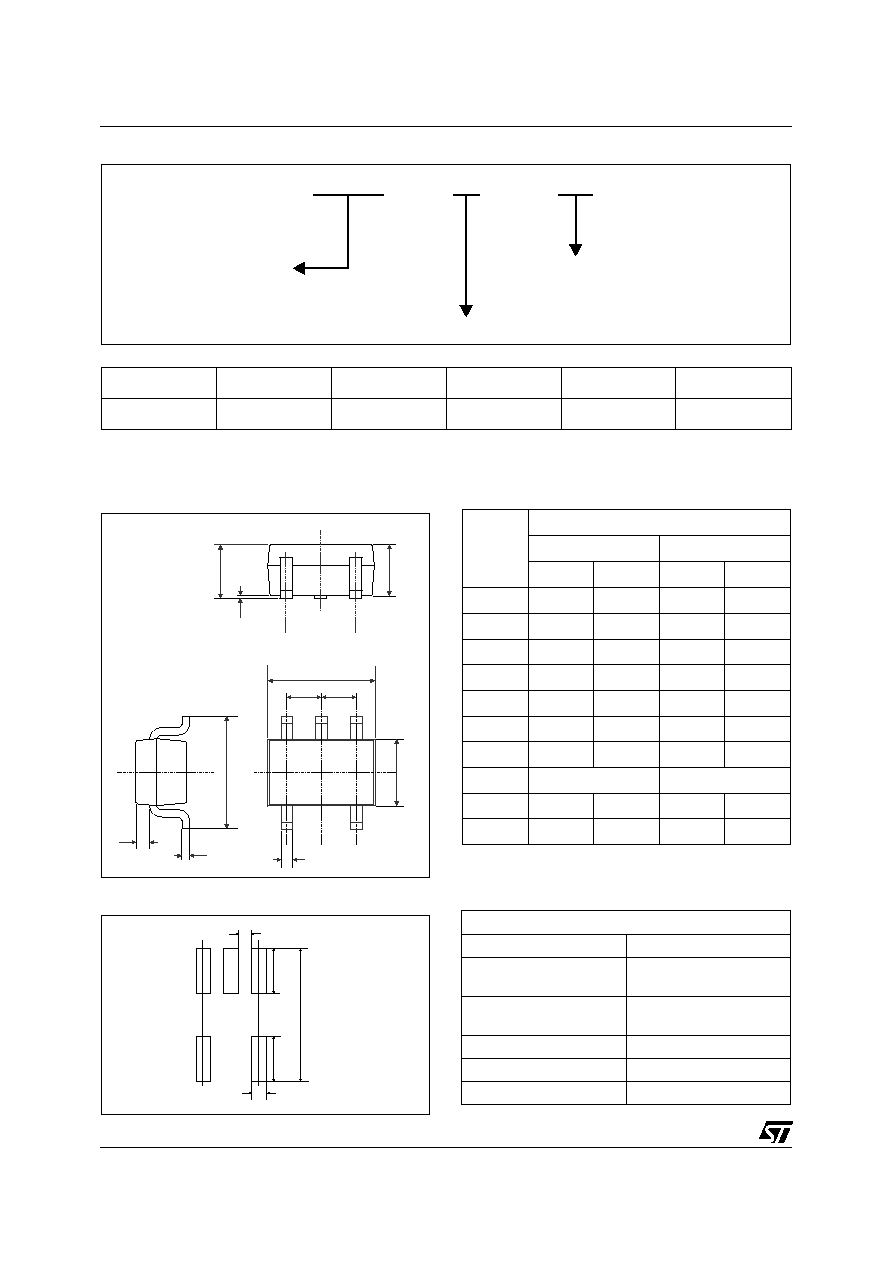
PACKAGE MECHANICAL DATA
SOT323-5L
E
c
Q1
H
b
D
A2
A
A1
e
e
REF.
DIMENSIONS
Millimeters
Inches
Min.
Max.
Min.
Max.
A
0.8
1.1
0.031
0.043
A1
0
0.1
0
0.004
A2
0.8
1
0.031
0.039
b
0.15
0.3
0.006
0.012
c
0.1
0.18
0.004
0.007
D
1.8
2.2
0.071
0.086
E
1.15
1.35
0.045
0.053
e
0.65 Typ.
0.026 Typ.
H
1.8
2.4
0.071
0.094
Q1
0.1
0.4
0.004
0.016
FOOT PRINT (in millimeters)
0.3mm
1mm
1mm
0.35mm
29mm
ESDA 25
W5
ESD ARRAY
Package: SOT323-5L
V min
BR
ORDER CODE
Mechanical specifications
Lead plating
Tin-lead
Lead plating thickness
5
µ
m min.
25
µ
m max.
Lead material
Sn / Pb
(70% to 90% Sn)
Lead coplanarity
10
µ
m max.
Body material
Molded epoxy
Epoxy meets
UL94,V0
Ordering type
Marking
Package
Weight
Base qty
Delivery mode
ESDA25W5
E25
SOT323-5L
5.4 mg.
3000
Tape & reel

ESDA25W5
5/5
Information furnished is believed to be accurate and reliable. However, STMicroelectronics assumes no responsibility for the consequences of
use of such information nor for any infringement of patents or other rights of third parties which may result from its use. No license is granted by
implication or otherwise under any patent or patent rights of STMicroelectronics. Specifications mentioned in this publication are subject to
change without notice. This publication supersedes and replaces all information previously supplied.
STMicroelectronics products are not authorized for use as critical components in life support devices or systems without express written ap-
proval of STMicroelectronics.
The ST logo is a registered trademark of STMicroelectronics
© 2000 STMicroelectronics - Printed in Italy - All rights reserved.
STMicroelectronics GROUP OF COMPANIES
Australia - Brazil - China - Finland - France - Germany - Hong Kong - India - Italy - Japan - Malaysia
Malta - Morocco - Singapore - Spain - Sweden - Switzerland - United Kingdom - U.S.A.
http://www.st.com