ESDA6V1FUx
Æ
November 1998 - Ed: 1
9-bit wide undershoot and overshoot clamping
functions.
Breakdown voltage : V
BR
= 6.1V min.
Forward voltage V
F
= 1.25V max. @ I
F
=200mA
Low capacitance: C =130pF @ V
RM
=5.25V.
Low clamping voltage.
200W peak pulse power (8/20
µ
s).
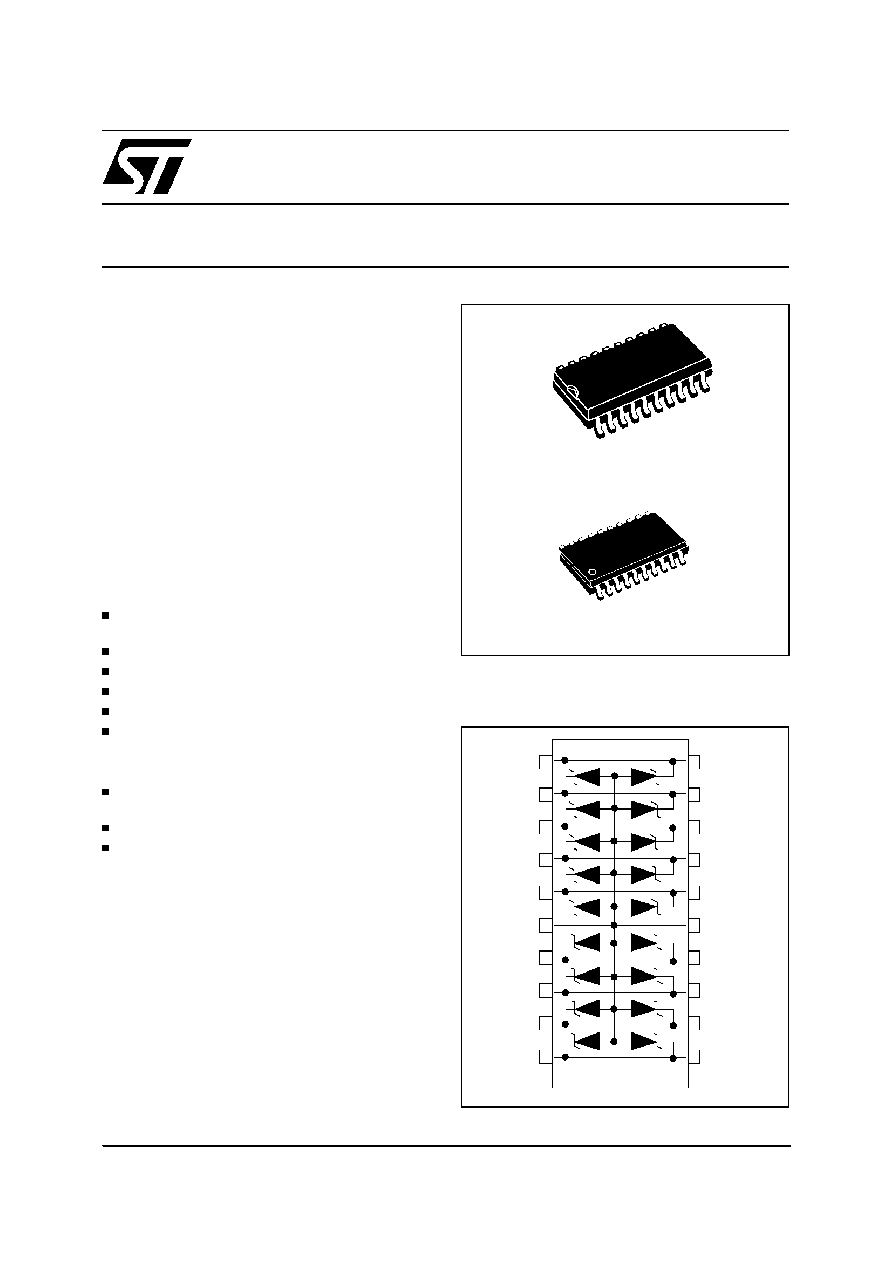
FEATURES
SSOP20
PIN-OUT CONFIGURATION
I1
O1
I2
O2
I3
O3
I4
O4
I5
O5
GND
GND
I6
O6
I7
O7
I8
O8
I9
O9
ESD protection of 25 kV, according to
MIL STD- Method 3015-6.
High integration.
Four points structure, avoiding all ESD effects
at the outputs.
BENEFITS
ESD PROTECTION MONOLITHIC
9-BIT WIDE TRANSIL
TM
ARRAY
Application Specific Discretes
A.S.D.
TM
Where protection in ESD sensitive equipmentis re-
quired, such as :
- Computers
- Printers
- Communication systems
MAIN APPLICATIONS
The ESDA6V1FUx is a monolithic TRANSIL array
designed to provide a 9-bit wide undershoot and
overshoot clamping function in association with
ESD protection level of up to 25 kV.
The ESDA6V1FUx provides best efficiency when
using separated inputs and outputs, in the so
called 4-point structure.
DESCRIPTION
SO20
TRANSIL is a trademark of STMicroelectronics
- ESD standard:
. IEC 1000-4-2
Level4
15kV
(air discharge)
8kV
(contactdischarge)
- MIL STD 883C - Method 3015-6
V
P
= 25 kV
C = 100 pF
R = 1500
3 positive strikes and 3 negative strikes (F = 1 Hz)
- Human body test :
V
P
= 4 kV
C = 150 pF
R = 150
COMPLIESWITH THE FOLLOWINGSTANDARDS :
1/7
Symbol
Parameter
Value
Unit
V
PP
Maximum electrostatic discharge in following measure-
ment conditions:
MIL STD 883C - METHOD 3015-6
IEC1000-4-2 - air discharge
IEC1000-4-2 - contact discharge
25
16
9
kV
P
PP
Peak pulse power (8/20
µ
s)
200
W
T
stg
T
j
Storage temperature
Maximum junction temperature
- 55 to + 150
125
∞
C
∞
C
ABSOLUTE MAXIMUM RATINGS (T
amb
=
25
∞
C)
Symbol
Parameter
V
RM
Stand-off voltage
V
BR
Breakdown voltage
V
CL
Clamping voltage
V
F
Forward voltage drop
C
Capacitance
Rd
Dynamic impedance
I
RM
Leakage current
I
PP
Peak pulse current
Symbol
Test conditions
Min.
Typ.
Max.
Unit
I
RM
V
RM
= 5.25 V, between any I/O pin and GND
20
µ
A
V
BR
I
R
= 1 mA, between any I/O pin and GND
6.1
7.2
V
V
F
IF = 200 mA, between any I/O pin and GND
1.25
V
Rd
I
PP
= 15 A, t
p
= 2.5
µ
s (note 1)
0.2
C
Between any I/O pin and GND at 0 V bias
Between any I/O pin and GND at V
RM
= 5.25 V
260
130
pF
Note 1 : see the calculation of the clamping voltage.
ESDA6V1FUx
2/7
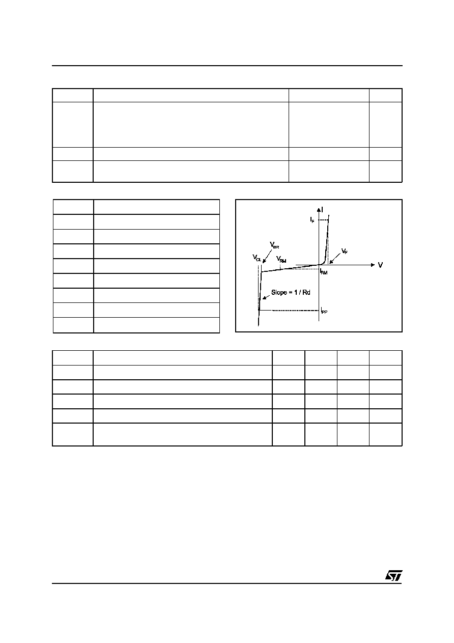
The ESDA family has been designed to clamp fast
spikes like ESD. Generally the PCB designers
need to calculate easily the clamping voltage V
CL
.
This is why we give the dynamic resistance in ad-
dition to the classical parameters. The voltage
across the protection cell can be calculated with
the following formula:
V
CL
= V
BR
+ Rd I
PP
Where Ipp is the peakcurrent throughthe ESDA cell.
DYNAMIC RESISTANCE MEASUREMENT
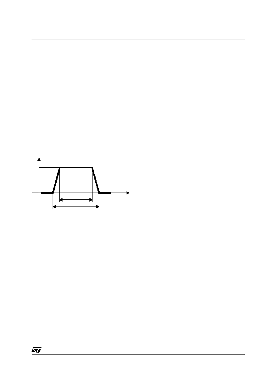
The short duration of the ESD has led us to prefer
a more adapted test wave, as below defined, to the
classical 8/20
µ
s and 10/1000
µ
s surges.
2.5
µ
s duration measurement wave.
As the value of the dynamic resistance remains
stable for a surge duration lower than 20
µ
s, the
2.5
µ
s rectangularsurge is well adapted. In addition
both rise and fall times are optimized to avoid any
parasitic phenomenon during the measurement of
Rd.
CALCULATION OF THE CLAMPING VOLTAGE
USE OF THE DYNAMIC RESISTANCE
2
µ
s
tp = 2.5
µ
s
t
I
Ipp
ESDA6V1FUx
3/7
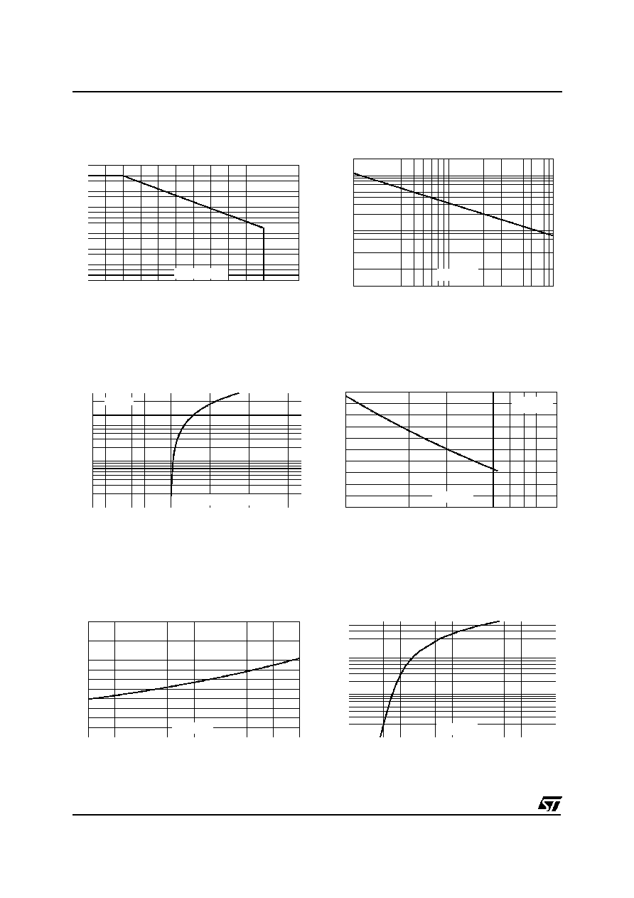
0
25
50
75
100
125
150
0.0
0.1
0.2
0.3
0.4
0.5
0.6
0.7
0.8
0.9
1.0
1.1
Ppp[Tj initial]/Ppp[Tj initial=25
∞
C]
Tj initial(
∞
C)
Fig 1: Peak power dissipation versus initial
junction temperature.
1
10
100
10
100
1000
2000
Ppp(W)
tp(
µ
s)
Fig 2: Peak pulse power versus exponential
pulse duration (Tj initial=25
∞
C).
4
5
6
7
8
9
10
11
12
0.1
1.0
10.0
30.0
Ipp(A)
tp=2.5
µ
s
Vcl(V) (output voltage)
Fig 3: Clamping voltage versus peak pulse current
(Tj initial=25
∞
C, rectangular waveform tp=2.5
µ
s).
1
2
5
10
100
120
140
160
180
200
C(pF)
F=1MHz
Vosc=30mV
VR(V)
Fig 4: Capacitance versus reverse applied
voltage (typical values).
25
50
75
100
125
0.0
0.5
1.0
1.5
2.0
2.5
3.0
IR[Tj] / IR[Tj=25
∞
C]
Tj(
∞
C)
Fig 5: Relative variation of leakage current
versus junction temperature (typical values).
0.6
0.8
1.0
1.2
1.4
1.6
1.8
0.01
0.10
1.00
5.00
IFM(A)
VFM(V)
Fig 6: Peak forward voltage drop versus peak
forward current (typical values).
Rectangular waveform: tp = 2.5
µ
s
ESDA6V1FUx
4/7
ESD protection by the ESDA6V1FUx
Electrostatic discharge (ESD) is a major cause of failure in electronic systems.
Transient Voltage Suppressors (TVS) are an ideal choice for ESD protection.They are capableof clamping
the incoming transient to a low enough level such that damage to the protected semiconductor is pre-
vented.
Surface mount TVS arrays offer the best choice for minimal lead inductance.
They serve as parallel protection elements, connected between the signal line to ground. As the transient
rises above the operatingvoltage of the device, the TVS array becomes a low impedance path diverting the
transient current to ground.
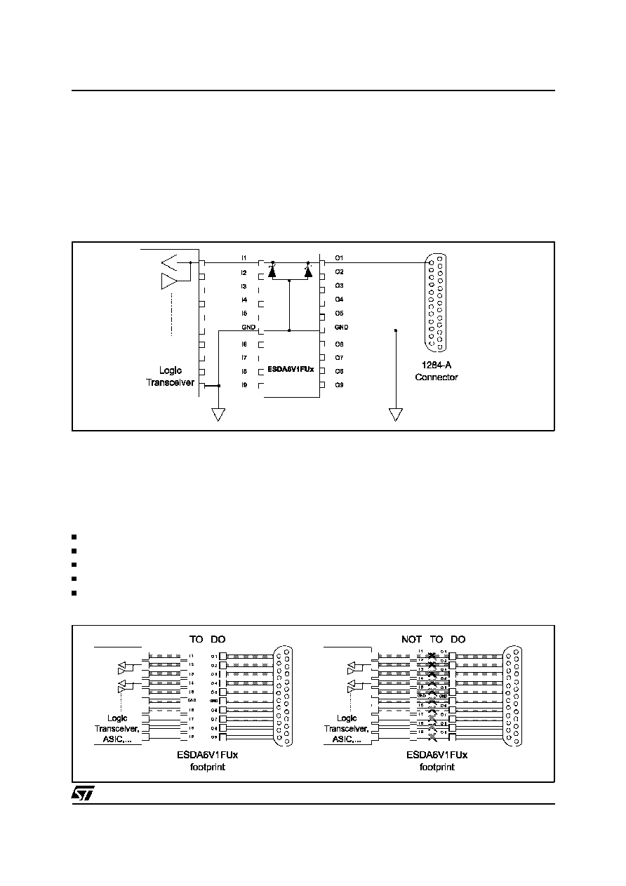
The ESDA6V1FUx array is the ideal board level protection of ESD sensitive semiconductor components.
It provides best efficiency when using separated inputs and outputs, in the so called 4-points structure.
Circuit Board Layout
Circuit board layout is a critical design step in the suppression of ESD induced transients. The following
guidelines are recommended :
The ESDA6V1FUx should be placed as near as possible to the input terminals or connectors.
The path length between the ESD suppressor and the protected line should be minimized.
All conductive loops, including power and ground loops should be minimized.
The ESD transient return path to ground should be kept as short as possible.
Ground planes should be used whenever possible.
Fig. 7 : Example of connection for one cell of the ESDA6V1FUx
Fig. 8 : Recommended PCB layout to benefit from 4 point structure
ESDA6V1FUx
5/7