 | –≠–ª–µ–∫—Ç—Ä–æ–Ω–Ω—ã–π –∫–æ–º–ø–æ–Ω–µ–Ω—Ç: ESDA6V1U1 | –°–∫–∞—á–∞—Ç—å:  PDF PDF  ZIP ZIP |
ESDA6V1U1
Æ
January 1998 - Ed : 2
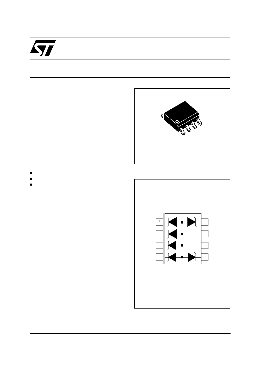
SO8
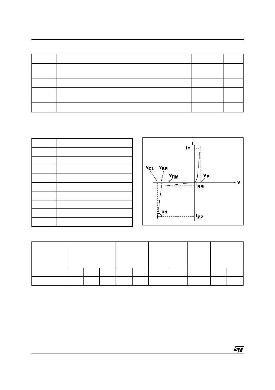
FUNCTIONAL DIAGRAM
2
3
4
I/O 1
I/O 2
I/O 3
I/O 4
I/O 6
G N D
G N D
I/O 5
8
7
6
5
TRANSIL
TM
ARRAY
FOR ESD PROTECTION
Application Specific Discretes
A.S.D.
TM
BENEFITS
High ESD protection level : up to 25 kV
High integration
Suitable for high density boards
IEC 1000-4-2 : level 4
MIL STD 883C-Method 3015-6 : class3
(human body model)
COMPLIES WITH THE FOLLOWING STANDARDS :
Where transient overvoltage protection in ESD
sensitive equipment is required, such as :
- COMPUTERS
- PRINTERS
- COMMUNICATION SYSTEMS
- GSM HANDSETS AND ACCESSORIES
- CAR RADIO
It is particulary recommended for parallel port
protection where the line interface withstands only
2 kV ESD surge.
APPLICATIONS
6 UNIDIRECTIONAL TRANSIL
TM
FUNCTIONS
LOW LEAKAGE CURRENT: I
R
max. < 2
µ
A
200 W PEAK PULSE POWER (8/20
µ
s)
FEATURES
DESCRITION
The ESDA6V1U1 is a monolithic voltage
suppressor designed to protect components which
are connected to data and transmission lines
against ESD.
It clamps the voltage just above the logic level
supply for positive transients, and to a diode drop
below ground for negative transients.
1/6
Symbol
Parameter
V
RM
Stand-off voltage
V
BR
Breakdown voltage
V
CL
Clamping voltage
I
RM
Leakage current
I
PP
Peak pulse current
T
Voltage temperature coefficient
C
Capacitance
Rd
Dynamic resistance
V
F
Forward voltage drop
ELECTRICAL CHARACTERISTICS (T
amb
= 25∞C)
Symbol
Parameter
Value
Unit
V
PP
Electrostatic discharge
MIL STD 883C - Method 3015-6
25
kV
P
PP
Peak pulse power (8/20
µ
s)
200
W
T
stg
T
j
Storage temperature range
Maximum junction temperature
- 55 to + 150
125
∞
C
∞
C
T
L
Maximum lead temperature for soldering during 10s
260
∞
C
ABSOLUTE MAXIMUM RATINGS (T
amb
= 25∞C)
Types
V
BR
@
I
R
I
RM
@ V
RM
Rd
T
C
V
F
@ I
F
min.
max.
max.
typ.
max.
typ.
max.
note 1
note 2
0V bias
V
V
mA
µ
A
V
10
-4
/
∞
C
pF
V
mA
ESDA6V1U1
6.1
7.2
1
2
5
0.5
6
100
1.5
200
note 1 : Square pulse, Ipp = 25A, tp=2.5
µ
s.
note 2 :
V
BR
=
T* (Tamb -25∞C) * V
BR
(25∞C)
ESDA6V1U1
2/6
The ESDA family has been designed to clamp fast
spikes like ESD. Generally the PCB designers
need to calculate easily the clamping voltage V
CL
.
This is why we give the dynamic resistance in
addition to the classical parameters. The voltage
across the protection cell can be calculated with
the following formula:
V
CL
= V
BR
+ Rd I
PP
Where Ipp is the peak current through the ESDA cell.
DYNAMIC RESISTANCE MEASUREMENT
The short duration of the ESD has led us to prefer
a more adapted test wave, as below defined, to the
classical 8/20
µ
s and 10/1000
µ
s surges.
2.5
µ
s duration measurement wave.
As the value of the dynamic resistance remains
stable for a surge duration lower than 20
µ
s, the
2.5
µ
s rectangular surge is well adapted. In addition
both rise and fall times are optimized to avoid any
parasitic phenomenon during the measurement of
Rd.
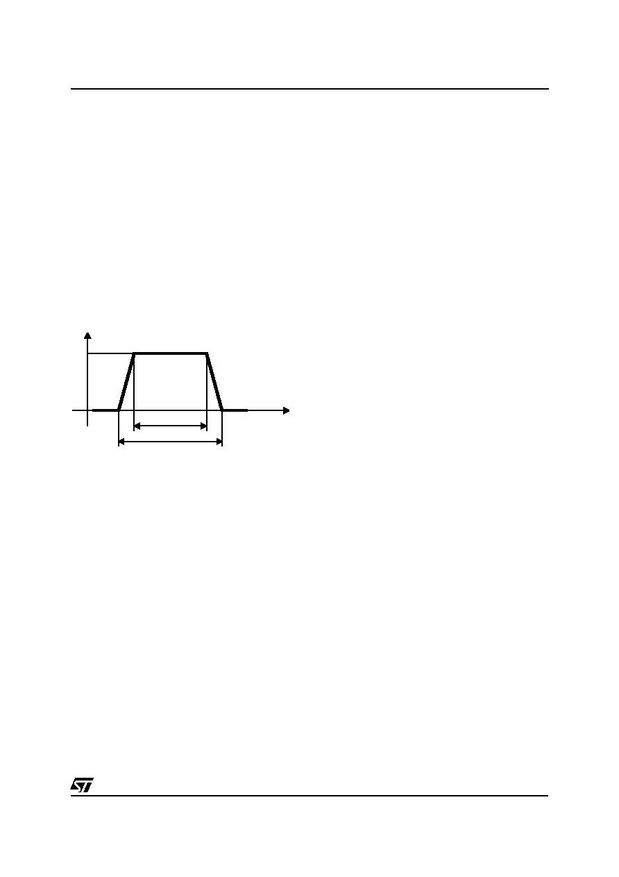
CALCULATION OF THE CLAMPING VOLTAGE
USE OF THE DYNAMIC RESISTANCE
2µs
tp = 2.5µs
t
I
Ipp
ESDA6V1U1
ESDA6V1U1
3/6
0
25
50
75
100
125
150
0.0
0.1
0.2
0.3
0.4
0.5
0.6
0.7
0.8
0.9
1.0
1.1
Ppp[Tj initial]/Ppp[Tj initial=25∞C]
Tj initial(∞C)
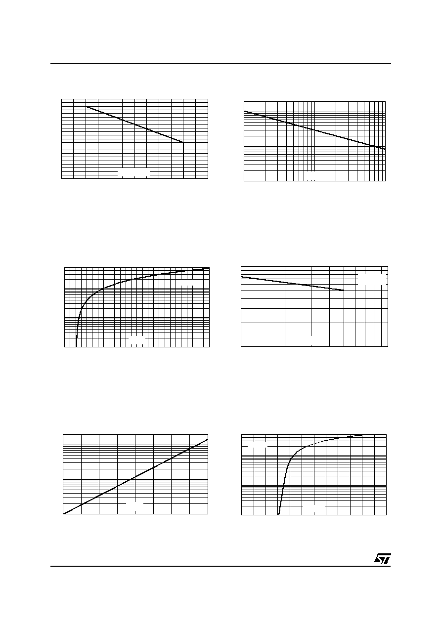
Fig. 1 : Peak power dissipation versus initial
junction temperature.
4
6
8
10 12 14 16 18 20 22 24 26 28 30
0.1
1.0
10.0
50.0
Ipp(A)
tp=2.5µs
V
(V)
CL
Fig. 3 : Clamping voltage versus peak pulse
current (Tj initial = 25 ∞C).
Rectangular waveform tp = 2.5
µ
s.
1
10
100
10
100
1000
2000
Ppp(W)
tp(µs)
Fig. 2 : Peak pulse power versus exponential
pulse duration (Tj initial = 25 ∞C).
25
50
75
100
125
1
10
100
200
I [Tj] / I [Tj=25∞C]
R
R
Tj(∞C)
Fig. 5 : Relative variation of leakage current
versus junction temperature (typical values).
0.0
0.5
1.0
1.5
2.0
2.5
3.0
0.01
0.10
1.00
5.00
I
(A)
FM
Tj=25∞C
V
(V)
FM
Fig. 6 : Peak forward voltage drop versus peak
forward current (typical values).
1
2
5
10
10
20
50
100
C(pF)
F=1MHz
Vosc=30mV
V (V)
R
Fig. 4 : Capacitance versus reverse applied
voltage (typical values).
ESDA6V1U1
4/6
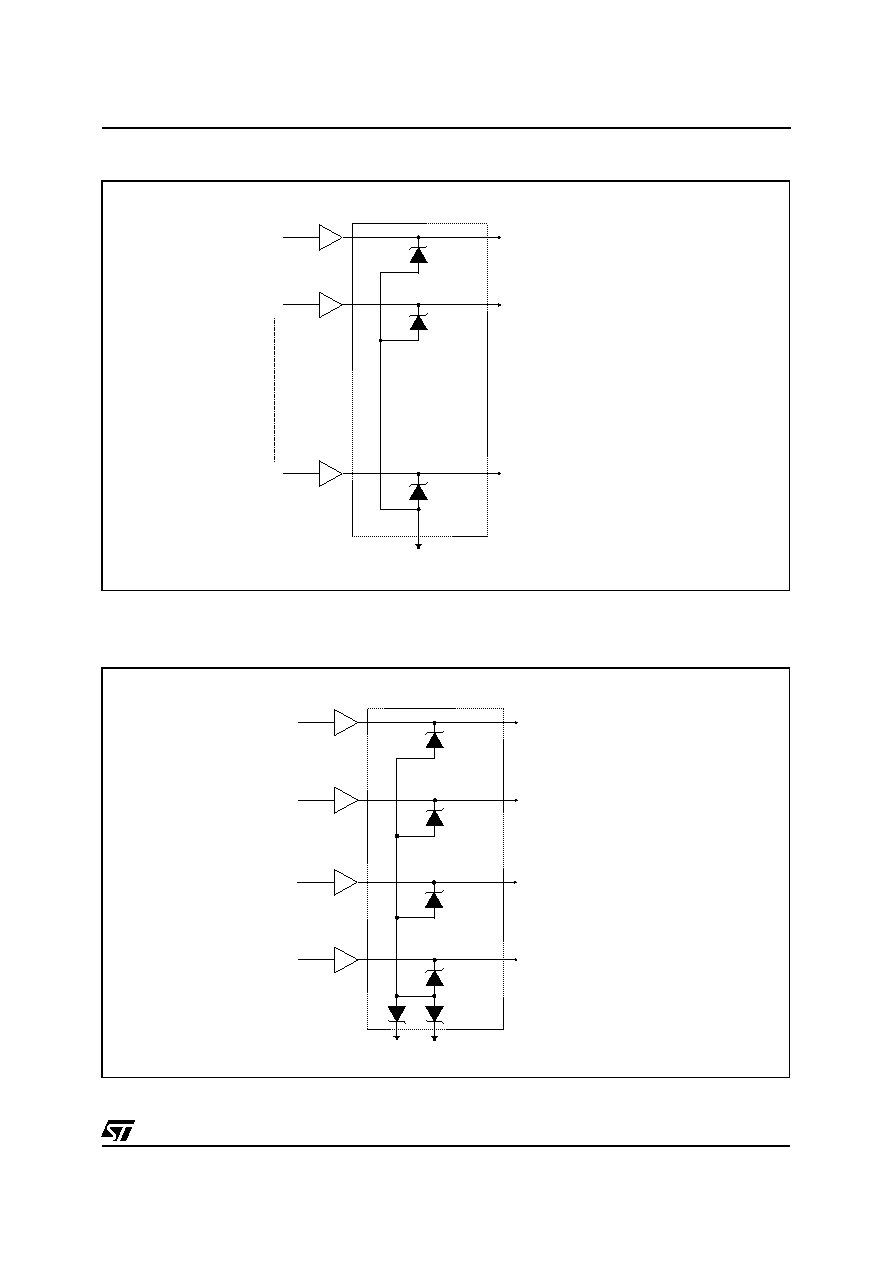
APPLICATION EXAMPLE : Protection of logic-level signals.
APPLICATION EXAMPLE : Protection of symmetrical signals.
Note : Capacitance value between any I/O pin and Ground is divided by 2.
D1
D2
Dn
0 to 5 V
0 to 5 V
0 to 5 V
ESDA6V1U1
A1
+/- 2.5 V
A2
+/- 2. 5 V
A4
+/- 2.5 V
A3
+/- 2.5 V
ESDA6V1U1
ESDA6V1U1
ESDA6V1U1
5/6