August 2006
Rev 1
1/7
ESDALC6V1C2
Quad low capacitance TRANSILTM array for ESD protection
Applications
Where transient overvoltage protection in ESD
sensitive equipment is required, such as:
Computers
Printers
Communication systems and cellular phones
Video equipment
This device is particularly adapted to the
protection of symmetrical signals
Features
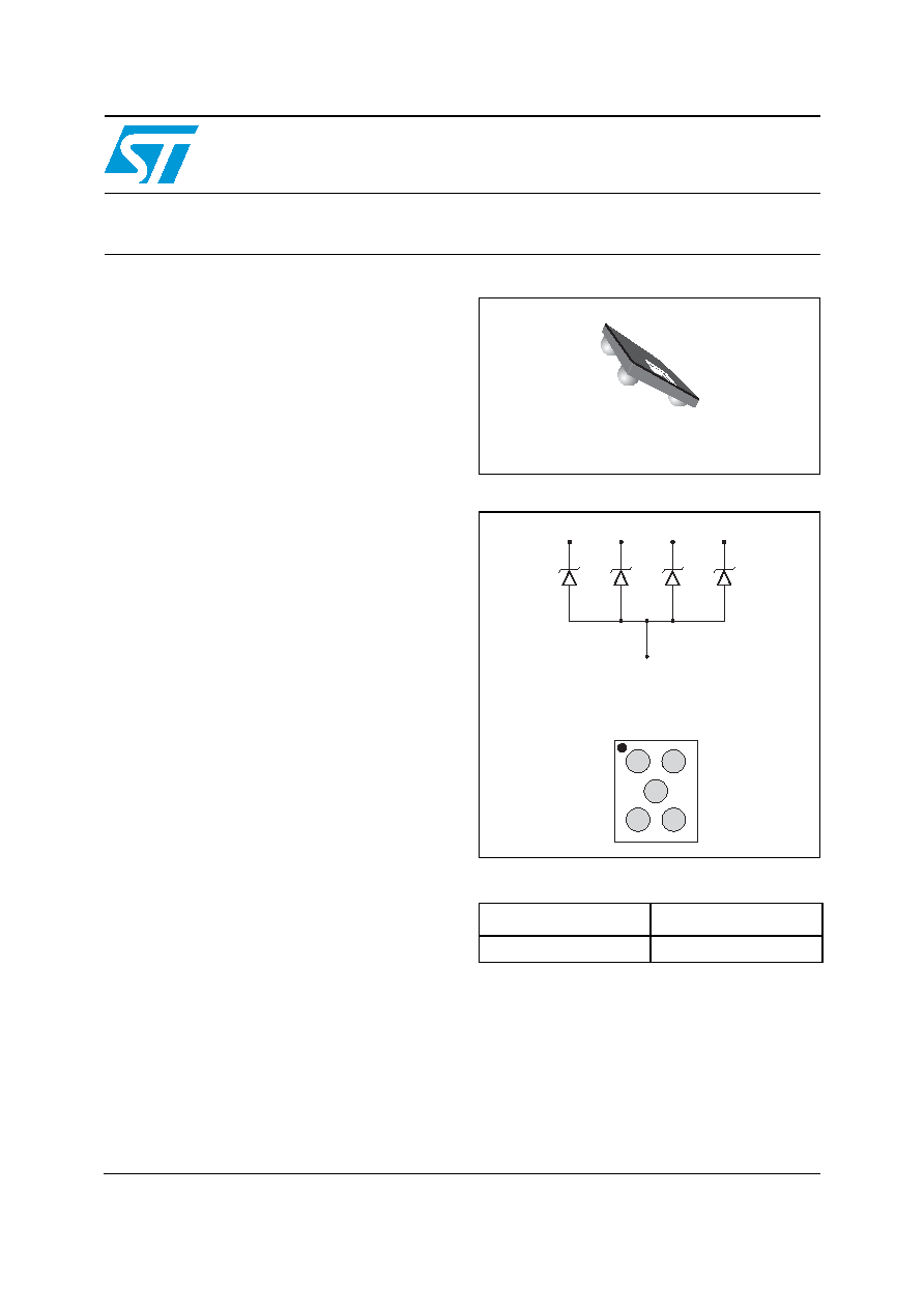
4 unidirectional TRANSIL functions.
Breakdown voltage V
BR
= 6.1 V min.
≠ Low diode capacitance (12 pF @ 0 V)
≠ Low leakage current (< 500 nA @ 3 V)
≠ very small PCB area (1.33 mm
2
)
Coated lead free package
Benefits
High ESD protection level
High integration
Suitable for high density boards
Description
The ESDALC6V1C2 is a monolithic array
designed to protect up to 4 lines againast ESD
transients. The device is ideal for applications
where both reduced line capacitance and board
space saving are required.
TM: TRANSIL is a trademark of STMicroelectronics
Functional diagram
Order code
Complies with the following standards:
Part number
Marking
ESDALC6V1C2
ED
IEC 61000-4-2
15 kV (air discharge)
8 kV (contact discharge)
MIL STD 883E - Method 3015-7: class 3
25 kV (Human body model)
Coated lead free Flip-Chip
(5 bumps)
B2
A1
A3
C1
C3
A B C
1
2
3
www.st.com

Characteristics
ESDALC6V1C2
2/7
1 Characteristics
Table 1.
Absolute maximum ratings (T
amb
= 25∞ C)
Symbol
Parameter
Value
Unit
V
PP
ESD discharge
IEC 61000-4-2 air discharge
IEC 61000-4-2 contact discharge
± 15
± 8
kV
P
PP
Peak pulse power dissipation (8/20 µs.
(1)
T
j initial
= T
amb
25
W
T
j
Junction temperature
125
∞C
T
stg
Storage temperature
- 55 to +150
∞C
T
L
Maximum lead temperature for soldering during 10 s at 5 mm for case
260
∞C
T
OP
Operating temperature range
- 40 to + 125
∞C
1.
For a surge greater than the maximum values, the diode will fail in short-circuit
Table 2.
Thermal resistance
Synbol
Parameter
Value
Unit
R
th(j-a)
Junction to ambient on printed circuit on recommended pad layout
150
∞C/W
Table 3.
Electrical characteristics
Symbol
Parameter
V
RM
Stand-of voltage
V
BR
Breakdown voltage
V
CL
Clamping voltage
I
RM
Leakage current @ V
RM
I
PP
Peak pulse current
T
Voltage temperature coefficient
V
F
Forward voltage drop
Type
I
RM
@ V
RM
V
BR
@ I
R
R
D
T
C
µA max
V
Vmin
Vmax
mA
Typ
10-4/∞C max pFtyp @0 V
ESDALC6V1C2
0.5
3
6.1
7.2
1
1
5
12
ESDALC6V1C2
Characteristics
3/7
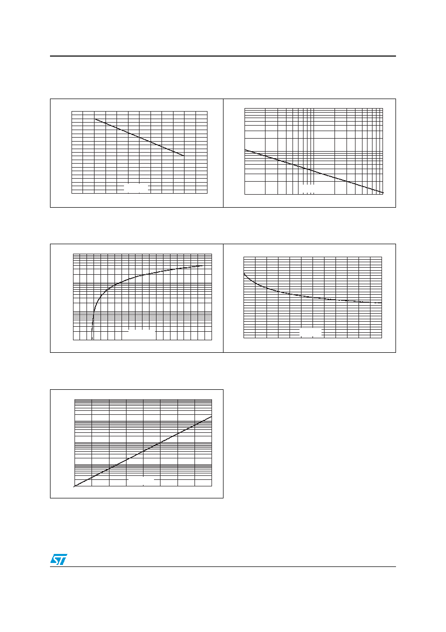
Figure 1.
Peak power dissipation versus
initial junction temperature
Figure 2.
Peak pulse power versus
exponential pulse duration
(T
j
initial = 25∞C)
0.0
0.1
0.2
0.3
0.4
0.5
0.6
0.7
0.8
0.9
1.0
1.1
0
25
50
75
100
125
150
P
PP
[T
j
initial] / P
PP
[T
j
initial=25∞C]
T
j
(∞C)
10
100
1000
1
10
100
P
PP
(W)
t
P
(µs)
Figure 3.
Clamping voltage versus peak
pulse current (T
j
initial = 25∞C),
rectangular waveform t
p
= 2.5 µs).
Figure 4.
Capacitance versus reverse applied
voltage (typical values)
Figure 5.
Relative variation of the leakage
current versus junction
temperature (typical values)
0.1
1.0
10.0
100.0
0
5
10
15
20
25
30
35
40
45
50
I
PP
(A)
V
CL
(V)
0
1
2
3
4
5
6
7
8
9
10
11
12
13
14
15
0
1
2
3
4
5
6
C(pF)
V
R
(V)
1.E+00
1.E+01
1.E+02
1.E+03
1.E+04
25
50
75
100
125
I
R
[T
j
] / I
R
[T
j
=25∞C]
T
j
(∞C)
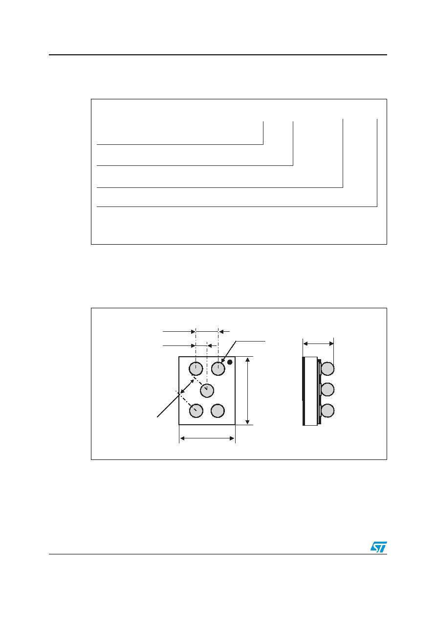
Ordering information scheme
ESDALC6V1C2
4/7
2
Ordering information scheme
3 Package
information
Figure 6.
Flip-Chip dimensions
ESDA LC - 6V1 C2
ESD Array
Low capacitance
VBR min = 6.1 V
Package
C = Coated Flip-Chip
2 = Leadfree Pitch = 500µm, Bump = 315µm
0.95 mm ± 50µm
1.32 mm ± 50µm
500 µm ± 15
315 µm ± 50
500 µm ± 10
250 µm ± 10
695 µm ± 65

ESDALC6V1C2
Ordering information
5/7
Figure 9.
Flip-Chip tape and reel specifications
In order to meet environmental requirements, ST offers these devices in ECOPACKÆ
packages. These packages have a lead-free second level interconnect. The category of
second level interconnect is marked on the package and on the inner box label, in
compliance with JEDEC Standard JESD97. The maximum ratings related to soldering
conditions are also marked on the inner box label. ECOPACK is an ST trademark.
ECOPACK specifications are available at: www.st.com.
4 Ordering
information
Figure 7.
Flip-Chip footprint
Figure 8.
Marking
Copper pad Diameter :
250µm recommended , 300µm max
Solder stencil opening : 330µm
Solder mask opening recommendation :
340µm min for 315µm copper pad diameter
Dot, ST logo
xx = marking
yww = datecode
(y = year ww = week)
z = manufacturing location
x
y
x
w
z
w
E
Dot identifying Pin A1 location
User direction of unreeling
All dimensions in mm
4 ± 0.1
8 ± 0.3
4 ± 0.1
1.75 ± 0.1
3.5 ± 0.1
ÿ 1.5 ± 0.1
0.73 ± 0.05
xxz
yww
ST
xxz
yww
ST
xxz
yww
ST
E
E
E
Part number
Marking
Package
Weight
Base qty
Delivery mode
ESDALC6V1C2
ED
Flip-Chip
2.1 mg
5000
Tape and reel