
Rev 3
January 2006
1/8
8
ESDALC6V1xxM6
4 and 5 line low capacitance TRANSILTM array for ESD protection
Main applications
Where transient overvoltage protection in ESD
sensitive equipment is required, such as:
Computers
Printers
Communication systems
Cellular phone handsets and accessories
Video equipment
Features
4 unidirectional TRANSIL diodes
(ESDALC6V1M6)
5 unidirectional TRANSIL diodes
(ESDALC6V1-5M6)
Breakdown Voltage V
BR
= 6.1 V min
Low diode capacitance (12 pF typ at 0 V)
Low leakage current < 70 nA
Very small PCB area: 1.45 mm
≤
500 microns pitch
Leadfree package
Description
The ESDALC6V1xxM6 is monolithic arrays
designed to protect up to 4 or 5 lines against ESD
transients.
The device is ideal for applications where both
reduced print circuit board space and power
absorption capability are required.
Benefits
High ESD protection level
High integration
Suitable for high density boards
Functional diagram
Order Code
Complies with the following standards:
TM: TRANSIL is a trademark of STMicroelectronics
Part number
Marking
ESDALC6V1M6
G
ESDALC6V1-5M6
H
IEC61000-4-2
15 kV
(air discharge)
8 kV
(contact discharge)
MIL STD 883E- Method 3015-7: class3
25 kV
(human body model)
Micro QFN Package
I/O1
I/O1
6
6
4
4
I/O5
I/O5
I/O3
I/O3
5
5
GND
GND
3
3
2
2
1
1
I/O2
I/O2
GND
I/O4
ESDALC6V1M6
ESDALC6V1-5M6
www.st.com
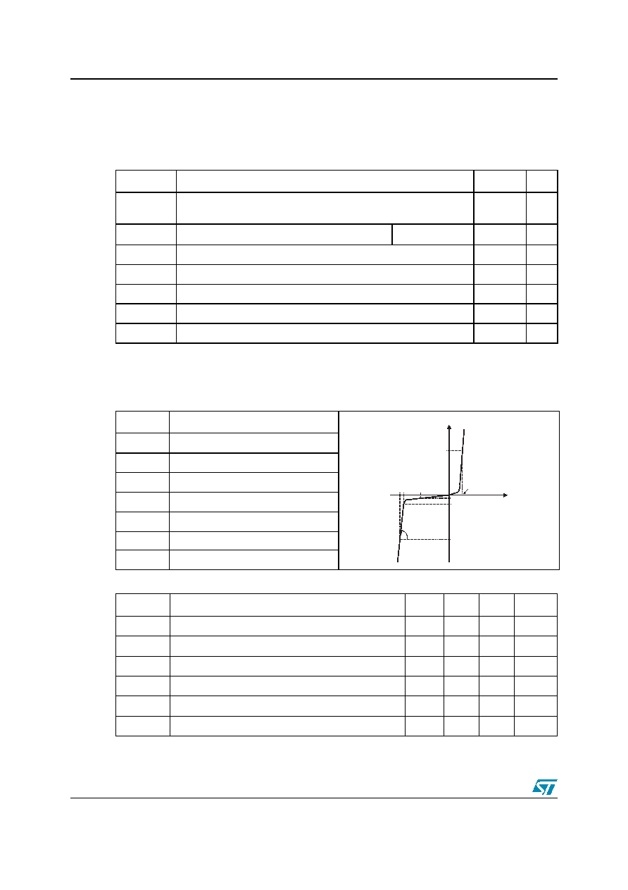
1 Characteristics
ESDALC6V1xxM6
2/8
1 Characteristics
1.1
Absolute maximum ratings (T
amb
= 25 ∞C)
1.2
Electrical characteristics (T
amb
= 25 ∞C)
Symbol
Parameter
Value
Unit
V
PP
ESD discharge ≠ IEC61000-4-2 air discharge
IEC61000-4-2 contact discharge
± 15
± 8
kV
P
PP
Peak pulse power dissipation (8/20 µs)
(1)
1.
For a surge greater than the maximum values, the diode will fail in short-circuit.
T
j
initial = T
amb
30
W
I
pp
Repetitive peak pulse current typical value (8/20 µs)
3
A
T
j
Junction temperature
125
∞C
T
stg
Storage temperature range
-55 + 150
∞C
T
L
Maximum lead temperature for soldering during 10 s
260
∞C
T
OP
Operating temperature range
-40 + 125
∞C
Symbol
Parameter
V
RM
Stand-off voltage
V
BR
Breakdown voltage
V
CL
Clamping voltage
I
RM
Leakage current @ V
RM
I
PP
Peak pulse current
T
Voltage temperature coefficient
V
F
Forward voltage drop
Parameter
Test Condition
Min
Typ
Max
Unit
V
BR
I
R
= 1 mA
6.1
7.2
V
I
RM
V
RM
= 3 V
70
nA
V
F
I
F
= 10 mA
1
V
R
d
2
3
T
(1)
1.
V
BR
=
T * (T
amb
- 25 ∞C) * V
BR
(25 ∞C)
I
R
= 1 mA,
5
10
-4
/∞C
C
V
R
=0 V DC, F
= 1 MHz, V
osc
= 30 mV
RMS
12
15
pF
V
V
V
I RM
I R
I PP
V
I
I F
V
V
Slope= 1/ Rd
V
V
CL
V
BR
RM
V
F
ESDALC6V1xxM6
1 Characteristics
3/8
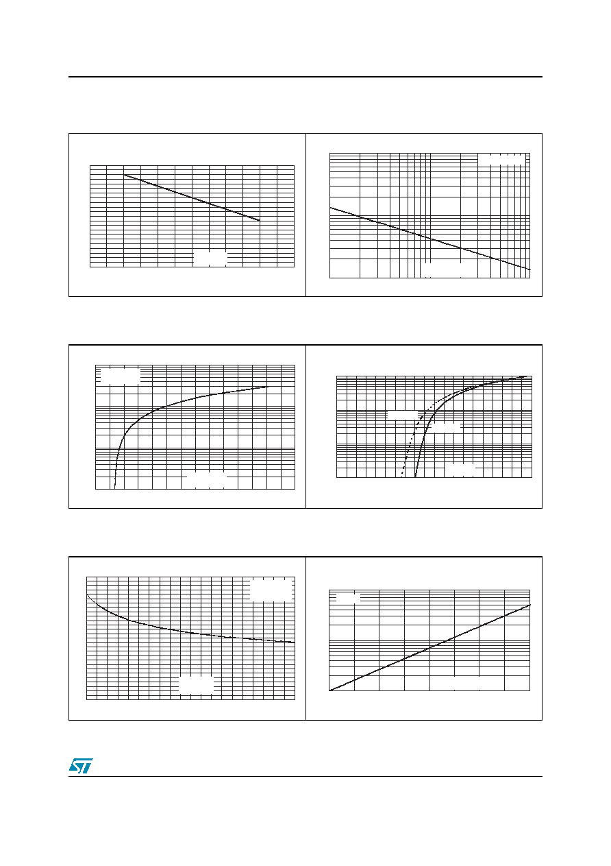
Figure 1.
Relative variation of peak pulse
power versus initial junction
temperature
Figure 2.
Peak pulse power versus
exponential pulse duration
Figure 3.
Clamping voltage versus peak pulse
current (typical values, rectangular
waveform)
Figure 4.
Forward voltage drop versus peak
forward current (typical values)
Figure 5.
Junction capacitance vesus reverse
voltage applied (typical values)
Figure 6.
Relative variation of leakage current
versus junction temperature (typical
values)
0.0
0.1
0.2
0.3
0.4
0.5
0.6
0.7
0.8
0.9
1.0
1.1
0
25
50
75
100
125
150
P
PP
[ T
j
i n it i al ] /P
PP
[ T
j
i n it i al = 2 5
]
T
j
(∞C)
∞C
10
100
1000
1
10
100
P
PP
(W)
T
j
initial = 25∞C
10
100
1000
1
10
100
P
PP
(W)
T
j
initial = 25∞C
t
P
(µs)
t
P
(µs)
0.1
1.0
10.0
100.0
0
10
20
30
40
50
60
70
I
PP
(A)
8/20µs
T
j
initial =25∞C
0.1
1.0
10.0
100.0
0
10
20
30
40
50
60
70
I
PP
(A)
8/20µs
T
j
initial =25∞C
V
CL
(V)
V
CL
(V)
1.E-03
1.E-02
1.E-01
1.E+00
0.0
0.2
0.4
0.6
0.8
1.0
1.2
1.4
1.6
1.8
2.0
I
F M
( A)
T
j
=25∞C
T
j
=125∞C
V
FM
(V)
C(pF)
C(pF)
0
1
2
3
4
5
6
7
8
9
10
11
12
13
14
0.0
0.5
1.0
1.5
2.0
2.5
3.0
3.5
4.0
4.5
5.0
F=1MHz
V
OSC
=30mV
RMS
T
j
=25∞C
V
R
(V)
V
R
(V)
1
10
100
25
50
75
100
125
I
R
[ T
j
] / I
R
[ T
j
= 2 5
]
V
R
=3V
∞C
T
j
(∞C)
1 Characteristics
ESDALC6V1xxM6
4/8
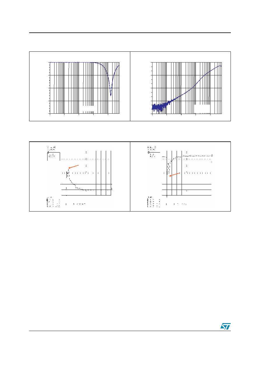
Figure 7.
S21 attenuation measurement
results of each channel
Figure 8.
Analog crosstalk measurements
between channels
Figure 9.
ESD response to IEC6100-4-2
(+15 kV air discharge) on each
channel
Figure 10. ESD response to IEC6100-4-2
(-15 kV air discharge) on each
channel
dB
100.0k
1.0M
10.0M
100.0M
1.0G
-40.00
-30.00
-20.00
-10.00
0.00
f/Hz
dB
100.0k
1.0M
10.0M
100.0M
1.0G
-120.00
-90.00
-60.00
-30.00
0.00
f/Hz
36V
-34V
-34V

ESDALC6V1xxM6
2 Ordering information scheme
5/8
2 Ordering
information
scheme
3 Package
information
Table 1.
Mechanical data
REF
DIMENSIONS
Millimeters
Inches
Min
Typ
Max
Min
Typ
Max
A
0.50 0.55
0.60
0.20
0.22
0.24
A1
0.00 0.02
0.05
0.00
0.01
0.02
b
0.19 0.25
0.30
0.07
0.10
0.12
D
1.34 1.45
1.51
0.53
0.57
0.59
E
0.94 1.00
1.05
0.37
0.39
0.41
e
0.45 0.50
0.55
0.18
0.20
0.22
k
0.25 0.30
0.35
0.10
0.12
0.14
L
0.30 0.35
0.40
0.12
0.14
0.16
ESDA LC 6V1 xx M6
ESD Array
Low capacitance
Package
M6 = Micro QFN 6 leads
Breakdown voltage
Number of lines
6V1 = 6.1 Volts min
blank = 4 line
-5 = 5 line protection
D
E
1
1
2
2
L
k
b
e
A
A1

3 Package information
ESDALC6V1xxM6
6/8
Figure 11. Footprint
Figure 12. Tape and reel specification
In order to meet environmental requirements, ST offers these devices in ECOPACKÆ
packages. These packages have a Lead-free second level interconnect . The category of
second level interconnect is marked on the package and on the inner box label, in compliance
with JEDEC Standard JESD97. The maximum ratings related to soldering conditions are also
marked on the inner box label. ECOPACK is an ST trademark. ECOPACK specifications are
available at: www.st.com.
0.50
0.25
0.30
0.65
1.60
Measurements in mm
4.00+/-0.1
1.
7
5
+/
-
0
.
1
4.00
1.5 +/- 0.1
3.
5
+
/
-
0.
0
3
User direction of unreeling
8.
0
+
/
-
0.
3
0.75
Dot identifying Pin A1 location
1.20
1.
6
5
2.0+/-0.05
X
X: Marking
X
X
4.00+/-0.1
1.
7
5
+/
-
0
.
1
4.00
1.5 +/- 0.1
3.
5
+
/
-
0.
0
3
User direction of unreeling
8.
0
+
/
-
0.
3
0.75
Dot identifying Pin A1 location
1.20
1.
6
5
2.0+/-0.05
X
X: Marking
X
X
X
X
ESDALC6V1xxM6
4 Ordering information
7/8
4 Ordering
information
5 Revision
history
Part number
Marking
Package
Weight
Base qty
Delivery mode
ESDALC6V1M6
G
Micro QFN
2.2 mg
30,000
Tape and reel
ESDALC6V1-5M6
H
Micro QFN
2.2 mg
30,000
Tape and reel
Date
Revision
Changes
19-Sep-2005
1
Initial release.
10-Oct-2005
2
Package title changed from DFN to QFN. No technical changes.
21-Dec-2005
3
Updated package dimensions in Table 1

5 Revision history
ESDALC6V1xxM6
8/8
Information furnished is believed to be accurate and reliable. However, STMicroelectronics assumes no responsibility for the consequences
of use of such information nor for any infringement of patents or other rights of third parties which may result from its use. No license is granted
by implication or otherwise under any patent or patent rights of STMicroelectronics. Specifications mentioned in this publication are subject
to change without notice. This publication supersedes and replaces all information previously supplied. STMicroelectronics products are not
authorized for use as critical components in life support devices or systems without express written approval of STMicroelectronics.
The ST logo is a registered trademark of STMicroelectronics.
All other names are the property of their respective owners
© 2006 STMicroelectronics - All rights reserved
STMicroelectronics group of companies
Australia - Belgium - Brazil - Canada - China - Czech Republic - Finland - France - Germany - Hong Kong - India - Israel - Italy - Japan -
Malaysia - Malta - Morocco - Singapore - Spain - Sweden - Switzerland - United Kingdom - United States of America
www.st.com