 | –≠–ª–µ–∫—Ç—Ä–æ–Ω–Ω—ã–π –∫–æ–º–ø–æ–Ω–µ–Ω—Ç: ESM1602 | –°–∫–∞—á–∞—Ç—å:  PDF PDF  ZIP ZIP |

ESM1602B
January 1996
QUAD COMPARATOR INTERFACE CIRCUIT
.
MINIMUM HYSTERESIS VOLTAGE AT EACH
INPUT : 0.3V
.
OUTPUT CURRENT : 15 mA
.
LARGE SUPPLY VOLTAGE RANGE : + 10V to
+ 35V
.
INTERNAL THERMAL PROTECTION
.
INPUT AND OUTPUT CLAMPING PROTEC-
TION DIODES.
DESCRIPTION
The ESM1602Bis a quadruplecomparatorintented
to provide an interface between signal processing
and transmitting lines in very noisy industrial sur-
roundings.
Outputof each comparator,used as line driver, sup-
plies a constant current (PNP output stage) and is
specially well protected against powerful overvol-
tages. The open collector output circuit allows the
connectionof several comparators to a single trans-
mitting line.
The ESM1602B can operate as receiver on a line
transmitting noisy high-voltage signals. Hysteresis
effect, internally implemented on inputs of each
comparator provides an excellent noise immunity.
In addition, each input is also protected against
overvoltages.
The ESM1602B can operate in a wide supply vol-
tage range (standard operational amplifier
±
15 V
supply or single + 12 V or + 24 V supplies used in
industrial electronic sets).
Moreover, internal thermal protection circuitry cuts
out the output current of the four comparators when
power dissipation becomes excessive.
DIP1 4
SO16
DIP14
SO16
1 - Inverting input 1
2 - Non-inverting input 1
3 - Output 1
4 - Non-inverting input 2
5 - Inverting input 2
6 - Output 2
7 - GND
8 - Output 3
9 - Inverting input 3
10 - Non-inverting input 3
11 - Output 4
12 - Non-inverting input 4
13 - Inverting input 4
14 - V
CC
1 - Inverting input 1
2 -Non-inverting input 1
3 - Output 1
4 - Non-inverting input 2
5 - Inverting input 2
6 - Output 2
7 - GND
8 - N.C.
9 - N.C.
10 - Output 3
11 - Inverting input 3
12 - Non-inverting input 3
13 - Output 4
14 - Non-inverting input 4
15 - Inverting input 4
16 - V
CC
ORDER ING NUMBERS: ESM1602B (DIP14)
ESM1602BFP (SO16)
PIN CONNECTIONS (to p view)
1/11
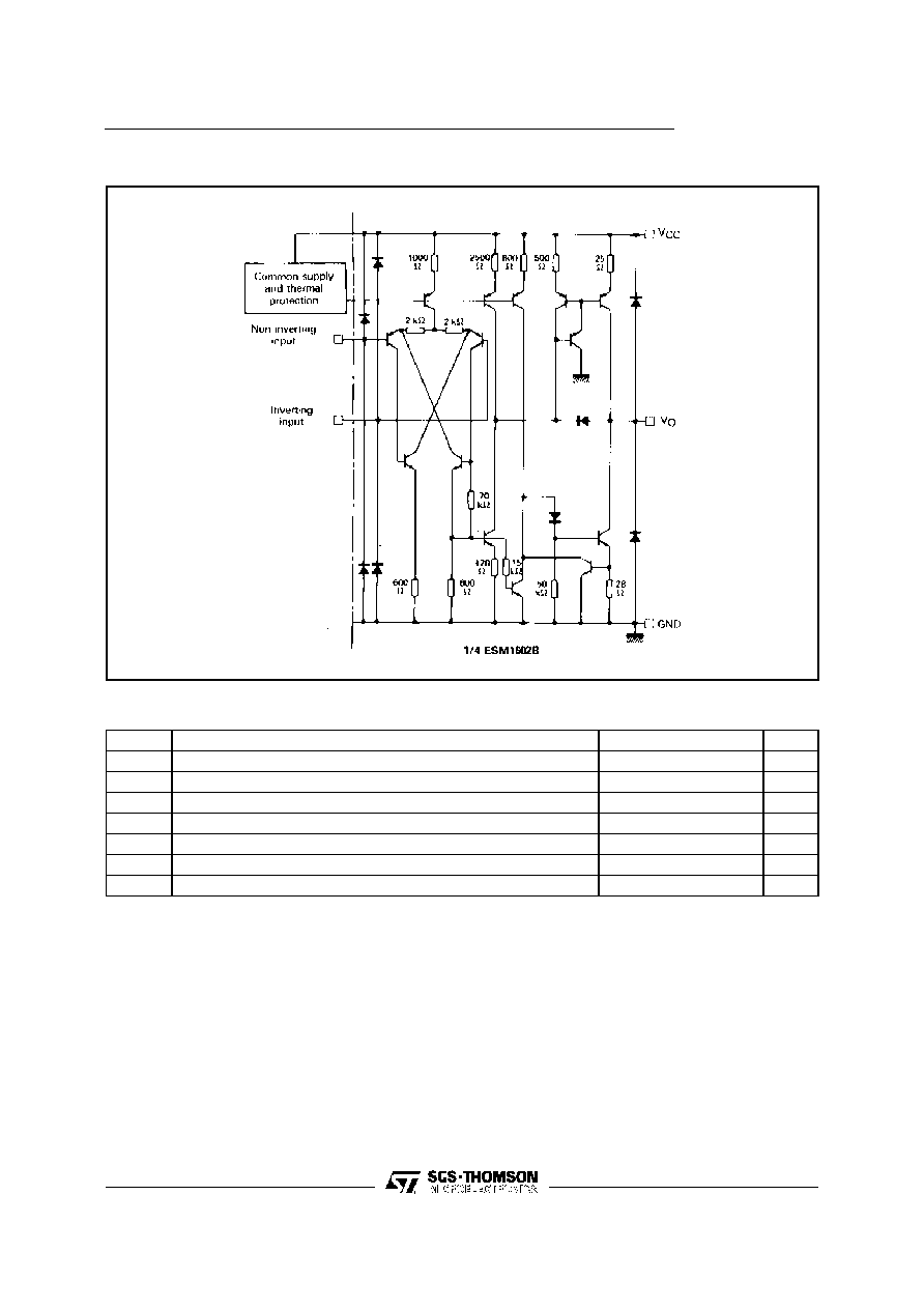
SCHEMATIC DIAGRAM
ABSOLUTE MAXIMUM RATINGS
Symbol
Parameter
Value
Unit
V
CC
Supply Voltage
45
V
V
ID
Differential Input Voltage
45
V
V
I
Input Voltage
≠0.7 to +45
V
I
O (max)
Output Current
Internally Limited
mA
P
tot
Power Dissipation
Internally Limited
W
T
op
Operating Ambient Temperature Range
≠25 to +85
o
C
T
stg
Storage Temperature Range
≠40 to +150
o
C
ESM1602B
2/11

ELECTRICAL CHARACTERISTICS
V
CC
= +35V, -25
o
C
T
amb
+85
o
C (unless otherwise specified)
Symbol
Parameter
Min.
Typ.
Max.
Typ.
Fig.
V
I
+
V
I
≠
Input Voltage Range - Note 1
Non-inverting Input
Inverting Input
0
2
33
33
V
V
V
C
Input Control Voltage (2V < V
CM
< 33V) - Note 2
150
500
mV
8
I
IB
Input Bias Current - Note 3
1
5
µ
A
I
SC
Short-circuit Output Current
V
CC
= +10 to +35 V
6
25
mA
9
V
CC
≠V
O
Output Saturation Voltage (high level) - (I
O
= ≠10mA)
1
1.5
V
11
V
O
Output Saturation Voltage (high level) - (I
O
= ≠10mA)
1
1.6
V
12
I
CC
Supply Current
R
L
=
for the 4 Comparators
R
L
Common for the 4 Comparators
4
10
6
13
mA
mA
13,14
S
VO
Output Slew-rate (R
L
= 3k
, T
amb
= +25
o
C)
1
V/
µ
s
V
F
Input Protective Diode Forward Voltage
(I = 20mA, T
amb
= +25
o
C)
1.5
V
≠
Energy of Pulses against which Circuit Output is Protected
(T
amb
= +25
o
C) - Note 4
20
mJ
≠
Pulsed Current Applied to Protective Output Diodes
(T
amb
= +25
o
C) - Note 5
0.4
A
15
No tes : 1. When negative input is biased between 0 and 2 volts output is always low.
2. Comparator hysteresis voltage on positive input on the one hand and negative input on the other hand equals sum of input control
voltages V
C1
+ V
C2
or V
C3
+ V
C4.
3. Input current flows out of the circuit owing to PNP input stage. This current is constant and independent of output level. So no load
change is transmitted to inputs.
4. By definition, a circuit is immunized against powerful signals when no durable character istic change occurs after the application of
these signals and when the circuit has not been destroyed.
In industrial surroundings, parasitic signals contain usually high voltage (over 200 V) AC harmonics having variable impedance of
500
to 10k
.
The power dissipation of thesesignals is divided between clamping diodes and the V
CC
. Simulationis used to determine the maximum
energy level. The injected current value cannot in any case exceed 3A.
5. Output protective diodes are tested individually by means of positive and negative dischar ge voltages of a capacitor. The negative
discharge control occurs through a single diode. During positive discharge, due to the properties of integration, a grounded collector
PNP transistor appears in parallel with the clamping diode connected to V
CC
. A part of the current flows through this transistor, V
CE
being greater than V
CC
. If T is the total discharge duration, energy dissipated in the circuit is :
For a certain injected current, the lower the current I
2
, that is to say the lower the PNP current gain the smaller the energy is dissipated in the cir-
cuit. Topology and technological processes have been chosen to shorten this current gain.
W =
T
[ i
1
vd +
i
2 (VCC + vd)
]
dt
O
ESM1602B
3/11

Figure 1: Input Bias Current
Figure 2: Output Saturation Voltage
Figure 3: Output Saturation Voltage
Figure 4: Short Circuit Current
ESM1602B
4/11
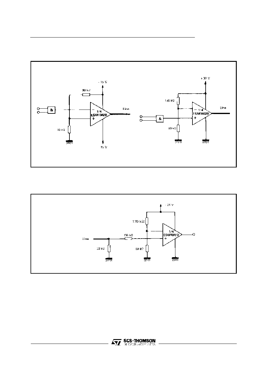
TYPICAL APPLICATIONS
Figure 5 : Conversion of DTL, TTL, MOS Signals on a Transmitting Line.
Figure 6 : Reception of Highly Noisy Signals.
ESM1602B
5/11

Figure 8.
Figure 7.
TEST CIRCUITS
ESM1602B
6/11

Figure 9.
Figure 10.
Figure 11.
Figure 12.
Figure 13.
Figure 14.
ESM1602B
7/11

Figure 15.
Figure 16: Response Time.
ESM1602B
8/11
DIP14 PACKAGE MECHANICAL DATA
Dimensions
Millimeters
Inches
Min.
Typ.
Max.
Min.
Typ.
Max.
a1
0.51
0.020
B
1.39
1.65
0.055
0.065
b
0.5
0.020
b1
0.25
0.010
D
20
0.787
E
8.5
0.335
e
2.54
0.100
e3
15.24
0.600
F
7.1
0.280
i
5.1
0.201
L
3.3
0.130
Z
1.27
2.54
0.050
0.100
DI
P
1
4
.
T
B
L
ESM1602B
9/11

S016 PACKAGE MECHANICAL DATA
Dimensions
Millimeters
Inches
Min.
Typ.
Max.
Min.
Typ.
Max.
A
1.75
0.069
a1
0.1
0.2
0.004
0.008
a2
1.6
0.063
b
0.35
0.46
0.014
0.018
b1
0.19
0.25
0.007
0.010
C
0.5
0.020
c1
45
o
(typ.)
D
9.8
10
0.386
0.394
E
5.8
6.2
0.228
0.244
e
1.27
0.050
e3
8.89
0.350
F
3.8
4.0
0.150
0.157
G
4.6
5.3
0.181
0.209
L
0.5
1.27
0.020
0.050
M
0.62
0.024
S
8
o
(max.)
SO
1
6
.
T
B
L
ESM1602B
10/11

Information furnished is believed to be accurate and reliable. However, SGS-THOMSON Microelectronics assumes no responsibility for
the consequences of use of such information nor for any infringement of patents or other rig hts of third parties which may result from its
use. No license is granted by implication or otherwise under any patent or patent rights of SGS-THOMSON Microelectronics. Specification
mentioned in this publication are subject to change without notice. This publication supe rsedes and replaces all information previously
supplied. SGS-THOMSON Microelectronics products are not authorized for use as critical components in life support devices or systems
without express written approval of SGS-THOMSON Microelectronics.
©
1997 SGS-THOMSON Microelectronics ≠ Printed in Italy ≠ All Rights Reserved
SGS-THOMSON Microelectronics GROUP OF COMPANIES
Australia - Brazil - Canada - China - France - Germany - Hong Kong - Italy - Japan - Korea - Malaysia - Malta - Morocco -
The Netherlands - Singapore - Spain - Sweden - Switzerland - Taiwan - Thailand - United Kingdom - U.S.A.
ESM1602B
11/11