Äîêóìåíòàöèÿ è îïèñàíèÿ www.docs.chipfind.ru
Preliminary Data
February 2006
Rev 1
1/28
28
STLC3085
Integrated Pots Interface
for Home Access Gateway and WLL
Features
Monochip SLIC optimised for WLL & VoIP
applications
Implement all key features of the borsht
function
Single supply (4.5 to 12V)
Built in DC/DC Converter controller
Soft battery reversal with programmable
transition time
On-hook transmission
Programmable off-hook detector threshold
Integrated ringing
Integrated ring trip
Parallel control interface (3.3V logic level)
Programmable constant current feed
Surface mount package
Integrated thermal protection
Dual gain value option
Automatic recognition flyback and buckboost
configuration
BCDIIIS 90V technology
-40 to +85°C operating range
Description
The STLC3085 is a SLIC device specifically
designed for WLL (Wireless Local Loop), and
ISDN Terminal Adaptors and VoIP applications.
One of the distinctive characteristic of this device
is the ability to operate with a single supply
voltage (from +4.5V to +12V) and self generate
the negative battery by means of an on chip DC/
DC converter controller that drives an external
MOS switch.
The battery level is properly adjusted depending
on the operating mode. A useful characteristic for
these applications is the integrated ringing
generator.
The control interface is a parallel type with open
drain output and 3.3V logic levels. Constant
current feed can be set from 20mA to 25mA.
Off-hook detection threshold is programmable
from 5mA to 9mA.
The device, developed in BCDIIIS technology
(90V process), operates in the extended
temperature range and integrates a thermal
protection that sets the device in power down
when Tj exceeds 140°C..
Order codes
(*) ECOPACK® (see
Section 5
)
TQFP44
Part number
Temp range,
°C
Package
Packing
E-STLC3085 (*)
-40 to 85
TQFP44
Tube
www.st.com

Contents
STLC3085
2/28
Contents
1
Block diagram and pin description . . . . . . . . . . . . . . . . . . . . . . . . . . . . . . . 3
1.1
Block diagram . . . . . . . . . . . . . . . . . . . . . . . . . . . . . . . . . . . . . . . . . . . . . . . . . 3
1.2
Pin connection . . . . . . . . . . . . . . . . . . . . . . . . . . . . . . . . . . . . . . . . . . . . . . . . 3
1.3
Pin description . . . . . . . . . . . . . . . . . . . . . . . . . . . . . . . . . . . . . . . . . . . . . . . . 4
1.4
Thermal data . . . . . . . . . . . . . . . . . . . . . . . . . . . . . . . . . . . . . . . . . . . . . . . . . . 5
2
Electrical specification . . . . . . . . . . . . . . . . . . . . . . . . . . . . . . . . . . . . . . . . . 6
2.1
Absolute maximum ratings . . . . . . . . . . . . . . . . . . . . . . . . . . . . . . . . . . . . . . . 6
2.2
Operating range . . . . . . . . . . . . . . . . . . . . . . . . . . . . . . . . . . . . . . . . . . . . . . . 6
2.3
Electrical characteristics . . . . . . . . . . . . . . . . . . . . . . . . . . . . . . . . . . . . . . . . . 7
3
Functional description . . . . . . . . . . . . . . . . . . . . . . . . . . . . . . . . . . . . . . . . 11
3.1
DC/DC converter . . . . . . . . . . . . . . . . . . . . . . . . . . . . . . . . . . . . . . . . . . . . . . 11
3.2
Operating modes . . . . . . . . . . . . . . . . . . . . . . . . . . . . . . . . . . . . . . . . . . . . . 12
3.2.1
Power down . . . . . . . . . . . . . . . . . . . . . . . . . . . . . . . . . . . . . . . . . . . . . . . . . . 12
3.2.2
High impedance feeding (HI-Z) . . . . . . . . . . . . . . . . . . . . . . . . . . . . . . . . . . . 12
3.2.3
Active . . . . . . . . . . . . . . . . . . . . . . . . . . . . . . . . . . . . . . . . . . . . . . . . . . . . . . . 13
3.2.4
Ringing . . . . . . . . . . . . . . . . . . . . . . . . . . . . . . . . . . . . . . . . . . . . . . . . . . . . . 14
3.2.5
Layout recommendation . . . . . . . . . . . . . . . . . . . . . . . . . . . . . . . . . . . . . . . . 16
3.2.6
External components list . . . . . . . . . . . . . . . . . . . . . . . . . . . . . . . . . . . . . . . . 16
4
Applications diagram . . . . . . . . . . . . . . . . . . . . . . . . . . . . . . . . . . . . . . . . . 20
Appendix A
STLC3085 test circuits . . . . . . . . . . . . . . . . . . . . . . . . . . . . . . . . . . . 21
Appendix B
STLC3085 overvoltage protection . . . . . . . . . . . . . . . . . . . . . . . . . . 24
Appendix C
Typical state diagram for STLC3085 operation . . . . . . . . . . . . . . . . 25
5
Package information . . . . . . . . . . . . . . . . . . . . . . . . . . . . . . . . . . . . . . . . . . 26
6
Revision history . . . . . . . . . . . . . . . . . . . . . . . . . . . . . . . . . . . . . . . . . . . . . . 27
STLC3085
Block diagram and pin description
3/28
1
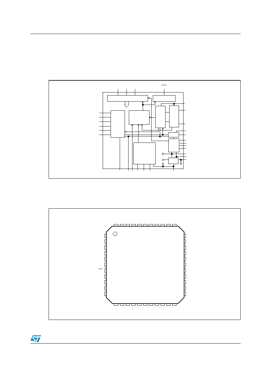
Block diagram and pin description
1.1 Block
diagram
Figure 1.
Block diagram
1.2 Pin
connection
Figure 2.
Pin connection
D0 D1 D2 DET
CAC ILTF RD IREF RLIM RTH
CSVR
CVCC
VPOS
BGND
TIP
RING
VBAT
AGND
TX
RX
ZAC1
ZAC
RS
ZB
SUPERVISION
AC PROC
REFERENCE
STAGE
LINE
DRIVER
CREV
INPUT LOGIC AND DECODER
OUTPUT LOGIC
VOLT.
Vcc
Vss
Agnd
OUTPUT
REG.
Status and functions
CLK
RSENSE
GATE
VF
DC/DC
CONV.
DC PROC
Vbat
1
2
3
5
6
4
7
8
9
10
17
11
18
19
20
21
22
44
43
42
41
39
40
38
37
36
35
34
28
27
26
24
23
25
33
32
31
29
30
N.C.
GAIN SET
PD
D1
D0
D2
RES
RES
RES
DET
RES
RES
RX
ZAC1
ZAC
ZB
RS
CAC
TX
CZ
VF
N.C.
VBAT1
CREV
N.C.
TIP
N.C.
N.C.
N.C.
RING
VBAT
BGND
RLIM
AGND
CVCC
RSENSE
GATE
CLK
VPOS
CSVR
ILTF
RD
IREF
RTH
D00TL488
12
13
14
15
16
Block diagram and pin description
STLC3085
4/28
1.3 Pin
description
Table 1.
Pin description
N°
Pin
Function
1
D0
Control Interface: input bit 0.
2
D1
Control Interface: input bit 1.
3
D2
Control interface: input bit 2.
4
PD
Power Down input. Normally connected to CVCC (or to logic level high).
5
Gain SET
Control gain interface:
0 Level R
xgain
= 0dB
T
xgain
= -6dB
1 Level R
xgain
= +6dB T
xgain
= -12dB
6,22,38,
39,40,42
NC
Not connected.
7
DET
Logic interface output of the supervision detector (active low).
8
RESERVED Connected to GND
9
RESERVED Connected to GND
10
RESERVED Connected to GND
11
RESERVED Left open.
12
RESERVED Connected to GND
13
RX
4 wire input port (RX input); 300K
input impedance. This signal is referred to AGND.
If connected to single supply CODEC output it must be DC decoupled with proper
capacitor.
14
ZAC1
RX buffer output (the AC impedance is connected from this node to ZAC).
15
ZAC
AC impedance synthesis.
16
RS
Protection resistors image (the image resistor is connected from this node to ZAC).
17
ZB
Balance Network for 2 to 4 wire conversion (the balance impedance ZB is connected from
this node to AGND. ZA impedance is connected from this node to ZAC1).
18
CAC
AC feedback input, AC/DC split capacitor (CAC).
19
TX
4 wire output port (TX output). The signal is referred to AGND. If connected to single
supply
CODEC input it must be DC decoupled with proper capacitor.
20
CZ
Fly-Back compensation
21
VF
Feedback input for DC/DC converter controller.
23
CLK
Power Switch Controller Clock (typ. 125KHz). This pin can also be connected to CVCC or
AGND. When the CLK pin is connected to CVCC an internal auto-oscillation is internally
generated and it is used instead of the external clock. When the CLK pin is connected to
AGND, the GATE output is disabled.
24
GATE
Driver for external Power MOS transistor (P-chanell in Buck-boost configuration, N-
channel in Fly-back configuration).
25
RSENSE
Voltage input for current sensing. RSENSE resistor should be connected close to this pin
and VPOS pin (Buck-boost) or GND (Fly-back). The PCB layout should minimize the
extra resistance introduced by the copper tracks.
STLC3085
Block diagram and pin description
5/28
1.4 Thermal
data
Table 2.
Thermal data
26
VPOS
Positive supply input.
27
CVCC
Internal positive voltage supply filter.
28
AGND
Analog Ground, must be shorted with BGND.
29
RLIM
Constant current feed programming pin (via RLIM). RLIM should be connected close to
this pin and AGND pin to avoid noise injection.
30
IREF
Internal bias current setting pin. RREF should be connected close to this pin and AGND
pin to avoid noise injection.
31
RTH
Off-hook threshold programming pin (via RTH). RTH should be connected close to this
pin and AGND pin to avoid noise injection.
32
RD
DC feedback and ring trip input. RD should be connected close to this pin and AGND pin
to avoid noise injection.
33
ILTF
Transversal line current image output.
34
CSVR
Battery supply filter capacitor.
35
BGND
Battery Ground, must be shorted with AGND.
36
VBAT
Regulated battery voltage self generated by the device via DC/DC converter.
Must be shorted to VBAT1.
37
RING
2 wire port; RING wire (Ib is the current sunk into this pin).
41
TIP
2 wire port; TIP wire (Ia is the current sourced from this pin).
43
CREV
Reverse polarity transition time control. A proper capacitor connected between this pin
and AGND is setting the reverse polarity transition time. This is the same transition time
used to shape the "trapezoidal ringing" during ringing injection.
44
VBAT1
Frame connection. Must be shorted to VBAT.
Symbol
Parameter
Value
Unit
R
th j-amb
Thermal Resistance Junction to Ambient
Typ.
60
°C/W
Table 1.
Pin description (continued)
N°
Pin
Function
Document Outline