 | –≠–ª–µ–∫—Ç—Ä–æ–Ω–Ω—ã–π –∫–æ–º–ø–æ–Ω–µ–Ω—Ç: ETC5064 | –°–∫–∞—á–∞—Ç—å:  PDF PDF  ZIP ZIP |
ETC5064/64-X
ETC5067/67-X
November 1994
POWER AMPLIFIER
SERIAL INTERFACE CODEC/FILTER WITH RECEIVE
ORDERING NUMBERS:
ETC5064FN
ETC5064FN-X
ETC5067FN
ETC5067FN-X
.
COMPLETE CODEC AND FILTERING SYS-
TEM INCLUDING :
-
Transmit high-pass and low-pass filtering.
-
Receive low-pass filter with sin x/x correction.
-
Active RC noise filter.
-
µ
-law or A-law compatible CODER and DE-
CODER.
-
Internal precision voltage reference.
-
Serial I/O interface.
-
Internal auto-zero circuitry.
-
Receive push-pull power amplifiers.
.
µ
-LAW ETC5064
.
A-LAW ETC5067
.
MEETS OR EXCEEDS ALL D3/D4 AND CCITT
SPECIFICATIONS.
.
±
5 V OPERATION.
.
LOW OPERATING POWER-TYPICALLY 70 mW
.
POWER-DOWN STANDBY MODE-TYPICALLY
3 mW
.
AUTOMATIC POWER DOWN
.
TTL OR CMOS COMPATIBLE DIGITAL INTER-
FACES
.
MAXIMIZES LINE INTERFACE CARD CIR-
CUIT DENSITY
.
0
∞
C TO 70
∞
C OPERATION: ETC5064/67
.
≠40
∞
C TO 85
∞
C OPERATION: ETC5064-X/67-X
DESCRIPTION
The ETC5064 (
µ
-law), ETC5067 (A-law) are mono-
lithic PCM CODEC/FILTERS utilizing the A/D and
D/A conversion architectureshown in the Block Dia-
grams and a serial PCM interface. The devices are
fabricated using double-poly CMOS process.
Similar to the ETC505X family, these devices fea-
ture an additional Receive Power Amplifier to pro-
vide push-pull balanced output drive capability. The
receive gain can be adjusted by means of two ex-
ternal resistors for an output level of up to
±
6.6 V
across a balanced 600
load.
Also included is an Analog Loopback switch and
TS
X
output.
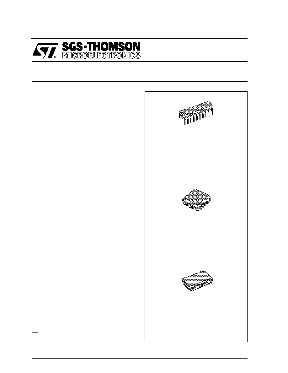
DIP20
(Plastic) N
PL CC20
FN
SO 20
D
ORDERING NUMBERS:
ETC5064N
ETC5064N-X
ETC5067N
ETC5067N-X
ORDERING NUMBERS:
ETC5064D
ETC5064D-X
ETC5067D
ETC5067D-X
1/18

BLOCK DIAGRAM (ETC5064 - ETC5064-X - ETC5067 - ETC5067-X)
PIN CONNECTIONS (Top views)
DI P20 &
SO20
PLCC20
ETC5064 - ETC5064-X - ETC5067 - ETC5067-X
2/18
PIN DESCRIPTION
Name
Pi n
Type (*)
N
Description
VPO
+
O
1
The Non-inverting Output of the Receive Power Amplifier
GNDA
GND
2
Analog Ground. All signals are referenced to this pin.
VPO
-
O
3
The Inverting Output of the Receive Power Amplifier
VPI
I
4
Inverting Input to the Receive Power Amplifier. Also powers down both
amplifiers when connected to V
BB
.
VF
R
O
O
5
Analog Output of the Receive Filter.
V
CC
S
6
Positive Power Supply Pin. V
CC
= +5V
±
5%
FS
R
I
7
Receive Frame Sync Pulse which enable BCLK
R
to shift PCM data into
D
R
. FS
R
is an 8KHz pulse train. See figures 1 and 2 for timing details.
D
R
I
8
Receive Data Input. PCM data is shifted into D
R
following the FS
R
leading
edge
BCLK
R
/CLKSEL
I
9
The bit Clock which shifts data into D
R
after the FS
R
leading edge. May
vary from 64KHz to 2.048MHz.
Alternatively, may be a logic input which selects either 1.536MHz/1.544MHz
or 2.048MHz for master clock in synchronous mode and BCLK
X
is used
for both transmit and receive directions (see table 1). This input has an
internal pull-up.
MCKL
R
/PDN
I
10
Receive Master Clock. Must be 1.536MHz, 1.544MHz or 2.048MHz. May
be asynchronous with MCLK
X
, but should be synchronous with MCLK
X
for
best performance. When MCLK
R
is connected continuously low, MCLK
X
is
selected for all internal timing. When MCLK
R
is connected continuously
high, the device is powered down.
MCLK
X
I
11
Transmit Master Clock. Must be 1.536MHz, 1.544MHz or 2.048MHz. May
be asynchronous with MCLK
R
.
BCLK
X
I
12
The bit clock which shifts out the PCM data on D
X
. May vary from 64KHz
to 2.048MHz, but must be synchronous with MCLK
X
.
D
X
O
13
The TRI-STAT E
Æ
PCM data output which is enabled by FS
X
.
FS
X
I
14
Transmit frame sync pulse input which enables BCLK
X
to shift out the
PCM data on D
X
. FS
X
is an 8KHz pulse train. See figures 1 and 2 for
timing details.
TS
X
O
15
Open drain output which pulses low during the encoder time slot. Must to
be grounded if not used.
ANLB
I
16
Analog Loopback Control Input. Must be set to logic '0' for normal
operation. When pulled to logic '1', the transmit filter input is disconnected
from the output of the transmit preamplifier and connected to the VPO
+
output of the receive power amplifier.
GS
X
O
17
Analog output of the transmit input amplifier. Used to set gain externally.
VF
X
I
-
I
18
Inverting input of the transmit input amplifier.
VF
X
I
+
I
19
Non-inverting input of the transmit input amplifier.
V
BB
S
20
Negative Power Supply Pin. V
BB
= -5V
±
5%
(*) I: Input, O: Output, S: Power Supply.
TRI- STATE
Æ
is a trademark of National Semiconductor Corp.
ETC5064 - ETC5064-X - ETC5067 - ETC5067-X
3/18

FUNCTIONAL DESCRIPTION
POWER-UP
When power is first applied, power-on reset circuitry
initializes the device and places it into the power-
down mode. All non-essential circuits are deacti-
vated and the D
X
and VF
R
O outputs are put in high
impedancestates. To power-up the device, a logical
low level or clock must be applied to the
MCLK
R
/PDN pin and FS
X
and/or FS
R
pulses must
be present. Thus 2 power-down control modes are
available. The first is to pull the MCLK
R
/PDN pin
high; the alternative is to hold both FS
X
and FS
R
in-
puts continuously low. The device will power-down
approximately 2 ms after the last FS
X
pulse. The
TRI-STATE PCM data output, D
X
, will remain in the
high impedance state until the second FS
X
pulse.
SYNCHRONOUS OPERATION
For synchronous operation, the same master clock
and bit clock should be used for both the transmit
and receive directions. In this mode, a clock must be
applied to MCLK
X
and the MCLK
R
/PDN pin can be
used as a power-down control. A low level on
MCLK
R
/PDN powers up the device and a high level
powers down the device. In either case, MCLKX will
be selected as the master clock for both the transmit
and receive circuits. A bit clock must also be applied
to BCLK
X
and the BCL
R
/CLKSEL can be used to se-
lect the proper internal divider for a master clock of
1.536 MHz, 1.544 MHz or 2.048 MHz. For 1.544
MHz operation, the device automatically compen-
sates for the 193 rd clock pulse each frame.
With a fixed level on the BCLK
R
/CKSEL pin, BCLK
X
will be selected as the bit clock for both the transmit
and receive directions. Table 1 indicates the fre-
quencies of operation which can be selected, de-
pending on the state of BCLK
R
/CLKSEL. In this syn-
chronous mode, the bit clock, BCLK
X
, may be from
64 kHz to 2.048 MHz, but must be synchronouswith
MCLK
X
.
Each FS
X
pulse begins the encoding cycle and the
PCM data from the previous encode cycle is shift out
of the enabled D
X
output on the positive edge of
BCLK
X
. After 8 bit clock periods, the TRISTATE D
X
output is returned to a high impedance state. With an
FS
R
pulse, PCM data is latched via the D
R
input on
the negativeedge of BCLK
X
(or on BCKL
R
if running).
FS
X
and FS
R
must be synchronous with MCLKX/
R
.
ASYNCHRONOUS OPERATION
For asynchronous operation, separate transmit and
receive clocks may be applied. MCLK
X
and MCLK
R
must be 2.048 MHz for the ETC5067 or 1.536 MHz,
1.544 MHz for the ETC5064, and need not be syn-
chronous. For best transmission performance, how-
ever, MCLK
R
should be synchronouswith MCLK
X
,
which is easily achieved by applyingonly static logic
levels to the MCLK
R
/PDN pin. This will automatically
connectMCLK
X
to all internal MCLK
R
functions(see
pin description). For 1.544 MHz operation, the de-
vice automatically compensates for the 193rd clock
pulse each frame. FS
X
starts each encoding cycle
and must be synchronous with MCLK
X
and BCLK
X
.
FS
R
starts each decoding cycle and must be syn-
chronous with BCLK
R
. BCLK
R
must be a clock, the
logic levels shown in Table 1 are not valid in asyn-
chronous mode. BCLK
X
and BCLK
R
may operate
from 64kHz to 2.048 MHz.
SHORT FRAME SYNC OPERATION
The device can utilize either a short frame sync
pulse or a long frame sync pulse.Upon power initiali-
zation, the device assumes a short frame mode. In
this mode, both frame sync pulses. FS
X
and FS
R
,
must be one bit clock period long, with timing rela-
tionships specified in figure 2. With FS
X
high during
a falling edge of BCLK
R
, the next rising edge of
BCLK
X
enables the D
X
TRI-STATE output buffer,
which will output the sign bit. The following seven ris-
ing edges clock out the remaining seven bits, and
the next falling edge disables the D
X
output. With
FS
R
high during a falling edge of BCLK
R
(BCLK
X
in
synchronous mode), the next falling edge of BCLK
R
latches in the sign bit. The following seven falling
edges latch in the seven remaining bits. Both de-
vices may utilize the short frame sync pulse in syn-
chronous or asynchronous operating mode.
LONG FRAME SYNC OPERATION
To use the long frame mode, both the frame sync
pulses, FS
X
and FS
R
, must be three or more bit clock
periods long, with timing relationships specified in
figure 3. Based on the transmit frame sync FS
X
, the
device will sense whether short or long frame sync
Table 1: Selection of Master Clock Frequencies.
BCLKR/CLKSEL
Master Clock
Frequency Selected
ETC5067
ETC5067-X
ETC5064
ETC5064-X
Clocked
2.048MHz
1.536MHz or
1.544MHz
0
1.536MHz or
1.544MHz
2.048MHz
1 (or open circuit)
2.048MHz
1.536MHz or
1.544MHz
ETC5064 - ETC5064-X - ETC5067 - ETC5067-X
4/18

pulses are being used. For 64 kHz operation, the
frame sync pulses must be kept low for a minimum
of 160 ns (see Fig 1). The D
X
TRI-STATE output
buffer is enabled with the rising edge of FS
X
or the
rising edge of BCLK
X
, whichever comes later, and
the first bit clocked out is the sign bit. The following
seven BCLK
X
rising edges clock out the remaining
seven bits. The D
X
output is disabled by the falling
BCLK
X
edge following the eighth rising edge, or by
FS
X
going low, whichever comes later. A rising edge
on the receive frame sync pulse, FS
R
, will cause the
PCM data at D
R
to be latched in on the next eight
falling edges of BCLK
R
(BCLK
x
in synchronous
mode). Both devices may utilize the long frame sync
pulse in synchronous or asynchronous mode.
TRANSMIT SECTION
The transmit section input is an operational amplifier
with provision for gain adjustment using two external
resistors, see figure 4. The low noiseand wide band-
width allow gains in excess of 20 dB across the
audio passband to be realized. The op amp drives
a unity gain filter consisting of RC active pre-filter,
followed by an eighth order switched-capacitor
bandpass filter directly drives the encoder sample-
and-hold circuit. The A/D is of companding type ac-
cording to A-law (ETC5067 and ETC5067-X) or
µ
-
law (ETC5064 and ETC5064-X) coding conven-
tions. A precision voltage reference is trimmed in
manufacturing to provide an input over load (t
MAX
)
of nominally 2.5V peak (see table of Transmission
Characteristics). The FS
X
frame sync pulse controls
the sampling of the filer output,and then the succes-
sive-approximationencodingcycle begins.The 8-bit
code is then loaded into a buffer and shifted out
throughD
X
at the next FS
X
pulse. the total encoding
delay will be approximately 165
µ
s (due to the trans-
mit filter) plus 125
µ
s (due to encoding delay), which
totals 290
µ
s. Any offset voltage due to the filters or
comparator is cancelled by sign bit integration.
RECEIVE SECTION
The receive section consist of an expanding DAC
which drives a fifth order switched-capacitor low
pass filter clocked at 256kHz. The decoder is A-law
(ETC5067 and ETC5067-X) or
µ
≠law (ETC5064
and ETC5064-X) and the 5 th order low pass filter
corrects for the sin x/x attenuation due to the 8kHz
sample and hold. The filter is then followed by a 2
nd order RC active post-filter and power amplifier
capable of driving a 600
load to a level of 7.2dBm.
The receive section is unity-gain. Upon the oc-
curence of FS
R
, the data at the D
R
input is clocked
in on the falling edge of the next eight BCLK
R
(BCKL
X
) periods.At the end of the decoder time slot,
the decoding cycle begins, and 10
µ
s later the de-
coder DAC output is updated.The total decoder de-
lay is about10
µ
s (decoder up-date) plus 110
µ
s (fil-
ter delay) plus 62.5
µ
s (1/2 frame), which gives ap-
proximately 180
µ
s.
RECEIVE POWER AMPLIFIERS
Two inverting mode power amplifiers are provided
for directly driving a matched line interface trans-
former. The gain of the first power amplifier can be
adjusted to boost the
±
2.5V peak output signal from
the receive filter up
±
3.3V peak into an unbalanced
300
load, or
±
4.0V into an unbalanced15k
load.
The second power amplifier is internally connected
in unity-gain inverting mode to give 6dB of signal
gain for balanced loads. Maximum power transfer to
a 600
subscriber line termination is obtained by
differientially driving a balanced transformer with a
2
: 1 turns ratio, as shown in figure 4. A total peak
power of 15.6dBm can be delivered to the load plus
termination. Both power amplifier can be powered
down independentlyfrom the PDN input by connect-
ing the VPI input to V
BB
saving approximately 12
mW of power.
ABSOLUTE MAXIMUM RATINGS
Symbol
Parameter
Valu e
Un it
V
CC
V
CC
to GNDA
7
V
V
BB
V
BB
to GNDA
-7
V
V
IN
, V
OUT
Voltage at any Analog Input or Output
V
CC
+0.3 to V
BB
-0.3
V
Voltage at any Digital Input or Output
V
CC
+0.3 to GNDA -0.3
V
T
oper
Operating Temperature Range: ETC5064/67
ETC5064-X/67-X
-25 to +125
-40 to +125
∞
C
∞
C
T
stg
Storage Temperature Range
-65 to +150
∞
C
Lead Temperature (soldering, 10 seconds)
300
∞
C
ETC5064 - ETC5064-X - ETC5067 - ETC5067-X
5/18
ELECTRICAL OPERATING CHARACTERISTICS
V
CC
= 5.0V
±
5%, V
BB
= -5V
±
5%, GNDA = 0V, T
A
= 0
∞
C to 70
∞
C (ETC5064-X/67-X: T
A
= ≠40
∞
C to 85
∞
), unless
otherwise noted; typical characteristics specified at V
CC
= 5.0V, V
BB
=-5.0V, T
A
= 25
∞
C; all signals are refer-
enced to GNDA.
DIGITAL INTERFACE (All devices)
Symbol
Parameter
Min.
Typ.
Max.
Unit
V
IL
Input Low Voltage
0.6
V
V
IH
Input High Voltage
2.2
V
V
OL
Output Low Voltage
I
L
= 3.2 mA
D
X
I
L
= 3.2 mA, Open Drain
TS
X
0.4
0.4
V
V
V
OH
Output High Voltage
IH = 3.2 mA
D
X
2.4
V
I
IL
Input Low Current (GNDA
V
IN
V
IL
)all digital inputs
Except BCLK
R
≠ 10
10
µ
A
I
IH
Input High Current (V
IH
V
IN
V
CC
) Except ANLB
≠ 10
10
µ
A
I
OZ
Output Current in High Impedance State (TRI-STAT E)
(GNDA
V
O
V
CC
)
D
X
≠ 10
10
µ
A
ANALOG INTERFACE WITH TRANSMIT INPUT AMPLIFIER (all devices)
Symbol
Parameter
Min.
Typ.
Max.
Unit
I
I
XA
Input Leakage Current
VFxI
+
or VFxI
≠
(≠ 2.5 V
V
+ 2.5 V)
≠ 200
200
nA
R
I
XA
Input Resistance
VF
X
I
+
or VF
X
I
≠
(≠ 2.5 V
V
+ 2.5 V)
10
M
R
O
XA
Output Resistance (closed loop, unity gain)
1
3
R
L
XA
Load Resistance
GS
X
10
k
C
L
XA
Load Capacitance
GS
X
50
pF
V
O
XA
Output Dynamic Range (R
L
10 k
)
GS
X
≠ 2.8
+2.8
V
A
V
XA
Voltage Gain (VF
X
I
+
to GS
X
)
5000
V/V
F
U
XA
Unity Gain Bandwidth
1
2
MHz
V
OS
XA
Offset Voltage
≠ 20
20
mV
V
CM
XA
Common-mode Voltage
≠ 2.5
2.5
V
CMRRXA
Common-mode Rejection Ratio
60
dB
PSRRXA
Power Supply Rejection Ratio
60
dB
ANALOG INTERFACE WITH RECEIVE FILTER (all devices)
Symbol
Parameter
Min.
Typ.
Max.
Unit
R
O
RF
Output Resistance
VF
R
O
1
3
R
L
RF
Load Resistance (VF
R
O =
±
2.5 V)
10
k
C
L
RF
Load Capacitance
25
pF
VOS
R
O
Output DC Offset Voltage
≠ 200
200
mV
ETC5064 - ETC5064-X - ETC5067 - ETC5067-X
6/18
ANALOG INTERFACE WITH POWER AMPLIFIERS (all devices)
Symbol
Parameter
Min.
Typ.
Max.
Unit
IPI
Input Leakage Current (≠ 1.0 V
VPI
1.0 V)
≠ 100
100
nA
RIPI
Input Resistance (≠ 1.0
VPI
1.0 V)
10
M
VIOS
Input Offset Voltage
≠ 25
25
mV
ROP
Output Resistance (inverting unity≠gain at VPO
+
or VPO
≠
)
1
F
C
Unity≠gain Bandwidth, Open Loop (VPO
≠
)
400
kHz
C
L
P
Load Capacitance (VPO
+
or VPO
≠
to GNDA)
R
L
1500
R
L
= 600
R
L
= 300
100
500
1000
pF
GAp
+
Gain VPO
≠
to VPO
+
to GNDA, Level at VPO
≠
= 1. 77 Vrms
(+ 3 dBmO)
≠ 1
V/V
PSRRp
Power Supply Rejection of V
CC
or V
BB
(VPO
≠
connected to VPI)
0 kHz ≠ 4 kHz
0 kHz ≠ 50 kHz
60
36
dB
POWER DISSIPATION (all devices)
Symbol
Parameter
Min.
Typ.
Max.
Unit
I
CC
0
Power-down Current at ETC6064/67
ETC5064-X/67-X
0.5
0.5
1.5
mA
mA
I
BB
0
Power-down Current at ETC6064/67
ETC5064-X/67-X
0.05
0.05
0.3
0.4
mA
mA
I
CC
1
Active Current at ETC6064/67
ETC5064-X/67-X
7.0
7.0
10.0
12.0
mA
mA
I
BB
1
Active Current at ETC6064/67
ETC5064-X/67-X
7.0
7.0
10.0
12.0
mA
mA
ELECTRICAL OPERATING CHARACTERISTICS (Continued)
ETC5064 - ETC5064-X - ETC5067 - ETC5067-X
7/18
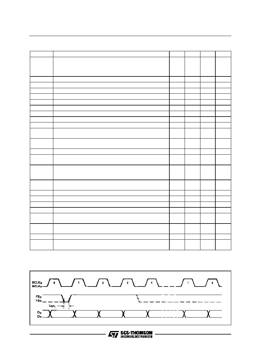
All TIMING SPECIFICATIONS
Symbol
Parameter
Min.
Typ.
Max.
Unit
1/t
PM
Frequency of master clocks
MCLK
X
and MCLK
R
Depends on the device used and the
BCLK
R
/CLKSEL Pin
1.536
2.048
1.544
MHz
t
WMH
Width of Master Clock High
MCLK
X
and MCLK
R
160
ns
t
WML
Width of Master Clock Low
MCLK
X
and MCLK
R
160
ns
t
RM
Rise Time of Master Clock
MCLK
X
and MCLK
R
50
ns
t
FM
Fall Time of Master Clock
MCLK
X
and MCLK
R
50
ns
t
PB
Period of Bit Clock
485
488
15.725
ns
t
WBH
Width of Bit Clock High (V
IH
= 2.2 V)
160
ns
t
WBL
Width of Bit Clock Low (V
IL
= 0.6 V)
160
ns
t
RB
Rise Time of Bit Clock (t
PB
= 488 ns)
50
ns
t
FB
Fall Time of Bit Clock (t
PB
= 488 ns)
50
ns
t
SBFM
Set-up time from BCLK
X
high to MCLK
X
falling edge.
(first bit clock after the leading edge of FS
X
)
100
ns
t
HBF
Holding Time from Bit Clock Low to the Frame Sync
(long frame only)
0
ns
t
SFB
Set-up Time from Frame Sync to Bit Clock (long frame only)
80
ns
t
HBFI
Hold Time from 3rd Period of Bit Clock
FS
X
or FS
R
Low to Frame Sync (long frame only)
100
ns
t
DZF
Delay Time to valid data from FS
X
or BCLK
X
, whichever
comes later and delay time from FSX to data output disabled
(C
L
= 0 pF to 150 pF)
20
165
ns
t
DBD
Delay Time from BCLK
X
high to data valid
(load = 150 pF plus 2 LSTTL loads)
0
150
ns
t
DZC
Delay Time from BCLK
X
low to data output disabled
50
165
ns
t
SDB
Set-up Time from D
R
valid to BCLK
R/X
low
50
ns
t
HBD
Hold Time from BCLK
R/X
low to D
R
invalid
50
ns
t
HOLD
Holding Time from Bit Clock High to Frame Sync (short frame only)
0
ns
t
SF
Set-up Time from FS
X/R
to BCLK
X/R
Low
(short frame sync pulse) - Note 1
80
ns
t
HF
Hold Time from BCLK
X/R
Low to FS
X/R
Low
(short frame sync pulse) - Note 1
100
ns
t
XDP
Delay Time to TS
X
low (load = 150 pF plus 2 LSTTI loads)
140
ns
t
WFL
Minimum Width of the Frame Sync Pulse (low level)
(64 bit/s operating mode)
160
ns
Note : 1.For short frame sync timing. FS
X
and FS
R
must go high while their respective bit clocks are
high.
Figure 1 : 64 k bits/s TIMING DIAGRAM. (see next page for complete timing)
ETC5064 - ETC5064-X - ETC5067 - ETC5067-X
8/18

Figure 2 : Short Frame Sync Timing.
ETC5064 - ETC5064-X - ETC5067 - ETC5067-X
9/18

Figure 3 : Long Frame Sync Timing.
ETC5064 - ETC5064-X - ETC5067 - ETC5067-X
10/18
TRANSMISSION CHARACTERISTICS
(all devices) T
A
= 0
∞
C to 70
∞
C (ETC5064-X/67-X: T
A
= ≠40
∞
C to 85
∞
), V
CC
= 5V
±
5%, V
BB
= ≠ 5V
±
5%,
GNDA = 0V, f = 1.02kHz, V
IN
= 0dBm0 transmit input amplifier connected for unity≠gainnon≠inverting.(unless
otherwise specified).
AMPLITUDE RESPONSE
Symbo l
Parameter
Min.
T yp.
Max.
Unit
Absolute Levels - Nominal 0 dBm0 is 4 dBm (600
).
0 dBm0
1.2276
Vrms
t
MAX
Max Overload Level
3.14 dBm0
ETC5067
3.17 dBm0
ETC5064
2.492
2.501
VPK
G
XA
Transmit Gain, Absolute (T
A
= 25
∞
C, V
CC
= 5V, V
BB
= -5V)
Input at GS
X
= 0dBm0 at 1020Hz
-0.15
0.15
dB
GXR
Transmit Gain, Relative to GXA
f = 16Hz
f = 50Hz
f = 60Hz
f = 180Hz
f = 200Hz
f = 300Hz -3000Hz
f = 3200Hz (ETC5064-X/67-X)
f = 3300Hz
f = 3400Hz
f = 4000Hz
f = 4600Hz and up, measure response from oHz to 4000Hz
-
-
-
-2.8
-1.8
-0.15
-0.35
-0.35
-0.7
-40
-30
-26
-0.2
-0.1
0.15
0.20
0.05
0
-14
-32
dB
G
XAT
Absolute Transmit Gain Variation with Temperature
T
A
= 0
∞
C to +70
∞
C
T
A
= ≠40
∞
C to +85
∞
C (ETC5064-X/67-X)
-0.1
-0.15
0.1
0.15
dB
G
XAV
Absolute Transmit Gain Variation with Supply Voltage
(V
CC
= 5V
±
5%, V
BB
= -5V
±
5%)
-0.05
0.05
dB
G
XRL
Transmit Gain Variation with Level
Sinusolidal Test Method Reference Level = -10dBm0
VF
X
I
+
= -40dBm0 to +3dBm0
VF
X
I
+
= -50dBm0 to -40dBm0
VF
X
I
+
= -55dBm0 to -50dBm0
-0.2
-0.4
-1.2
0.2
0.4
1.2
dB
G
RA
Receive Gain, Absolute (T
A
= 25
∞
C, V
CC
= 5V, V
BB
= -5V)
Input = Digital Code Sequence for 0dBm0 Signal at 1020Hz
-0.15
0.15
dB
G
RR
Receive Gain, Relative to G
RA
f = 0Hz to 3000Hz
f = 3200Hz (ETC5064-X/67-X)
f = 3300Hz
f = 3400Hz
f = 4000Hz
-0.15
-0.35
-0.35
-0.7
0.15
0.20
0.05
0
-14
dB
G
RAT
Absolute Receive Gain Variation with Temeperature
T
A
= 0
∞
C to +70
∞
C
T
A
= ≠40
∞
C to +85
∞
C (ETC5064-X/67-X)
-0.1
-0.15
0.1
0.15
dB
G
RAV
Absolute Receive Gain Variation with Supply Voltage
(V
CC
= 5V
±
5%, V
BB
= -5V
±
5%)
-0.05
0.05
dB
G
RRL
Receive Gain Variation with Level
Sinusoidal Test Method; Reference Input PCM code
corresponds to an ideally encoded -10dBm0 signal
PCM level = -40dBm0 to +3dBm0
PCM level = -50dBm0 to -40dBm0
PCM level = -55dBm0 to -50dBm0
-0.2
-0.4
-1.2
0.2
0.4
1.2
dB
V
RO
Receive Filter Output at VF
R
O R
L
= 10K
-2.5
2.5
V
ETC5064 - ETC5064-X - ETC5067 - ETC5067-X
11/18

TRANSMISSION CHARACTERISTICS (continued).
ENVELOPE DELAY DISTORTION WITH FREQUENCY
Symbol
Parameter
Min.
Typ.
Max.
Unit
D
XA
Transmit Delay, Absolute (f = 1600 Hz)
290
315
µ
s
D
XR
Transmit Delay, Relative to D
XA
f = 500 Hz-600 Hz
f = 600 Hz-800 Hz
f = 800 Hz-1000 Hz
f = 1000 Hz-1600 Hz
f = 1600 Hz-2600Hz
f = 2600 Hz-2800 Hz
f = 2800 Hz-3000 Hz
195
120
50
20
55
80
130
220
145
75
40
75
105
155
µ
s
D
RA
Receive Delay, Absolute (f = 1600 Hz)
180
200
µ
s
D
RR
Receive Delay, Relative to D
RA
f = 500 Hz-1000 Hz
f = 1000 Hz-1600 Hz
f = 1600 Hz-2600 Hz
f = 2600 Hz-2800 Hz
f = 2800 Hz-3000 Hz
≠ 40
≠ 30
≠ 25
≠ 20
70
100
145
90
125
175
µ
s
NOISE
Symbol
Parameter
Min.
Typ.
Max.
Unit
N
XP
Transmit Noise, P Message (A-LAW, VF
X
I
+
= 0 V) Weighted
1)
ETC5064
ETC5064-X
≠ 74
≠ 74
≠ 69
≠ 67
dBm0p
dBm0p
N
RP
Receive Noise, P Message Weighted
(A-LAW, PCM Code Equals Positive Zero)
≠ 82
≠ 79
dBm0p
N
XC
Transmit Noise, C Message Weighted
(
µ
-LAW, VFxI
+
= 0 V)
ETC5064
ETC5064-X
12
12
15
16
dBrnC0
dBrnC0
N
RC
Receive Noise, C Message Weighted
(
µ
-LAW, PCM Code Equals Alternating Positive and Negative Zero)
8
11
dBrnC0
N
RS
Noise, Single Frequency
f = 0 kHz to 100 kHz, Loop around Measurement, VF
X
I
+
= 0 V
≠ 53
dBm0
PPSR
X
Positive Power Supply Rejection, Transmit (note 2)
V
CC
= 5.0 V
DC
+ 100 mVrms, f = 0 kHz-50 kHz
40
dBp
NPSR
X
Negative Power Supply Rejection, Transmit (note 2)
V
BB
= 5.0 V
DC
+ 100 mVrms, f = 0 kHz-50 kHz
40
dBp
PPSR
R
Positive Power Supply Rejection, Receive (PCM code equals
positive zero, V
CC
= 5.0 V
DC
+ 100 mVrms)
f = 0 Hz-4000Hz
A LAW
µ
LAW
f = 4 kHz-25 kHz
f = 25 kHz-50 kHz
40
40
40
36
dBp
dBc
dB
dB
NPSR
R
Negative Power Supply Rejection, Receive (PCM code equals
positive zero, V
BB
= ≠ 5.0 V
DC
+ 100 mVrms)
f = 0 Hz-4000Hz
A LAW
µ
LAW
f = 4 kHz-25 kHz
f = 25 kHz-50 kHz
40
40
40
36
dBp
dBc
dB
dB
SOS
Spurious out-of-band Signals at the Channel Output
0 dBm0, 300 Hz-3400 Hz input PCM applied at D
R
4600 Hz-7600 Hz
7600 Hz-8400 Hz
8400 Hz-100,000 Hz
≠32
≠40
≠32
dB
dB
dB
ETC5064 - ETC5064-X - ETC5067 - ETC5067-X
12/18

TRANSMISSION CHARACTERISTICS (continued).
DISTORTION
Symbol
Parameter
Min.
Typ.
Max.
Unit
STD
X
or
STD
R
Signal to Total Distortion (sinusoidal test method)
Transmit or Receive Half-channel
Level = 3.0 dBm0
= 0 dBm0 to ≠ 30 dBm0
= ≠ 40 dBm0
XMT
RCV
= ≠ 55 dBm0
XMT
RCV
33
36
29
30
14
15
dBp
(ALAW)
dBc
(
µ
LAW)
SFD
X
Single Frequency Distortion, Transmit (T
A
= 25
∞
C)
≠ 46
dB
SFD
R
Single Frequency Distortion, Receive (T
A
= 25
∞
C)
≠ 46
dB
IMD
Intermodulation Distortion
Loop Around Measurement, VF
X
I
+
= ≠ 4 dBm0 to
≠ 21 dBm0, two Frequencies in the Range 300 Hz-3400 Hz
≠ 41
dB
CROSSTALK
Symbol
Parameter
Min.
Typ.
Max.
Unit
CT
X-R
Transmit to Receive Crosstalk, 0dBm0 Transmit
f = 300 Hz-3400 Hz, D
R
= Steady PCM Code
ETC5064/67
ETC5064-X/67-X
≠ 90
≠ 75
≠ 65
dB
dB
CT
R-X
Receive to Transmit Crosstalk, 0dBm0 Receive Level (note 2)
f = 300 Hz-3400 Hz, VF
X
I = 0 V
ETC5064/67
ETC5064-X/67-X
≠ 90
≠ 70
≠ 65
dB
dB
POWER AMPLIFIERS
Symbol
Parameter
Min.
Typ.
Max.
Unit
V
OL
Maximum 0 dBm0 Level for Better than
±
0.1 dB Linearity Over
the Range 10 dBm0 to + 3 dBm0
(balanced load, R
L
connected between VPO
+
and VPO
≠
)
R
L
= 600
R
L
= 1200
R
L
= 30 k
33
3.5
4.0
Vrms
S/D
P
Signal/Distortion R
L
= 600
, 0 dBm0
50
dB
Notes :
1. Measured by extrapolation from the distortion test results.
2. PPSRX, NPSRX, CTR≠X measured with a ≠50dBm0 activating signal applied at VF
X
I
+
ENCODING FORMAT AT D
X
OUTPUT
A-Law
(Including even bit inversion)
µ
Law
V
IN
(at GS
X
) = + Full-scale
1 0 1 0 1 0 1 0
1 0 0 0 0 0 0 0
V
IN
(at GS
X
) = 0 V
1 1 0 1 0 1 0 1
0 1 0 1 0 1 0 1
1 1 1 1 1 1 1 1
0 1 1 1 1 1 1 1
V
IN
(at GS
X
) = ≠ Full-scale
0 0 1 0 1 0 1 0
0 0 0 0 0 0 0 0
ETC5064 - ETC5064-X - ETC5067 - ETC5067-X
13/18

APPLICATION INFORMATION
POWER SUPPLIES
While the pins at the ETC506X family are well pro-
tected against electrical misure, it is recommended
that the standard CMOS practice be followed, en-
suring that ground is connected to the device before
any other connections are made. In applications
where the printed circuit board may be plugged into
a "hot" socket with power and clocks already pre-
sent, an extra long ground pin in the connector
should be used.
All ground connections to each device should meet
at a common point as close as possible to the GNDA
pin. This minimizes the interaction of ground return
currents flowing through a common bus impedance.
0.1
µ
F supply decoupling capacitors should be con-
nected from this common ground point to VCC and
VBB as close to the device as possible.
For best performance, the ground point of each
CODEC/FILTER on a card should be connected to
a common card ground in star formation, rather than
via a ground bus. This common ground point should
be decoupled to VCC and VBB with 10
µ
F capaci-
tors.
For best performance, TSx should be grounded if
not used.
Figure 4 : Typical Asynchronous Application.
ETC5064 - ETC5064-X - ETC5067 - ETC5067-X
14/18
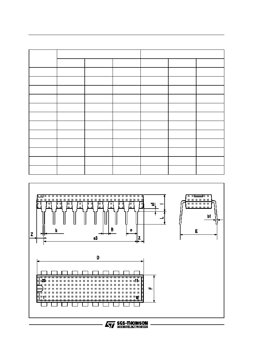
SO20 PACKAGE MECHANICAL DATA
DIM.
mm
inch
MIN.
TYP.
MAX.
MIN.
TYP.
MAX.
A
2.65
0.104
a1
0.1
0.2
0.004
0.008
a2
2.45
0.096
b
0.35
0.49
0.014
0.019
b1
0.23
0.32
0.009
0.013
C
0.5
0.020
c1
45
∞
(typ.)
D
12.6
13.0
0.496
0.510
E
10
10.65
0.394
0.419
e
1.27
0.050
e3
11.43
0.450
F
7.4
7.6
0.291
0.300
L
0.5
1.27
0.020
0.050
M
0.75
0.030
S
8
∞
(max.)
ETC5064 - ETC5064-X - ETC5067 - ETC5067-X
15/18
PLCC20 PACKAGE MECHANICAL DATA
DIM.
mm
inch
MIN.
TYP.
MAX.
MIN.
TYP.
MAX.
A
9.78
10.03
0.385
0.395
B
8.89
9.04
0.350
0.356
D
4.2
4.57
0.165
0.180
d1
2.54
0.100
d2
0.56
0.022
E
7.37
8.38
0.290
0.330
e
1.27
0.050
e3
5.08
0.200
F
0.38
0.015
G
0.101
0.004
M
1.27
0.050
M1
1.14
0.045
ETC5064 - ETC5064-X - ETC5067 - ETC5067-X
16/18
DIP20 PACKAGE MECHANICAL DATA
DIM.
mm
inch
MIN.
TYP.
MAX.
MIN.
TYP.
MAX.
a1
0.254
0.010
B
1.39
1.65
0.055
0.065
b
0.45
0.018
b1
0.25
0.010
D
25.4
1.000
E
8.5
0.335
e
2.54
0.100
e3
22.86
0.900
F
7.1
0.280
I
3.93
0.155
L
3.3
0.130
Z
1.34
0.053
ETC5064 - ETC5064-X - ETC5067 - ETC5067-X
17/18

Information furnished is believed to be accurate and reliable. However, SGS-THOMSON Microelectronics assumes no responsibility for
the consequences of use of such information nor for any infringement of patents or other rights of third parties which may result from its
use. No license is granted by implication or otherwise under any patent or patent rights of SGS-THOMSON Microelectronics. Specifica-
tions mentioned in this publication are subject to change without notice. This publication supersedes and replaces all information pre-
viously supplied. SGS-THOMSON Microelectronics products are not authorized for use as critical components in life support devices or
systems without express written approval of SGS-THOMSON Microelectronics.
©
1994 SGS-THOMSON Microelectronics - All Rights Reserved
SGS-THOMSON Microelectronics GROUP OF COMPANIES
Australia - Brazil - France - Germany - Hong Kong - Italy - Japan - Korea - Malaysia - Malta - Morocco - The Netherlands - Singapore -
Spain - Sweden - Switzerland - Taiwan - Thaliand - United Kingdom - U.S.A.
ETC5064 - ETC5064-X - ETC5067 - ETC5067-X
18/18