 | –≠–ª–µ–∫—Ç—Ä–æ–Ω–Ω—ã–π –∫–æ–º–ø–æ–Ω–µ–Ω—Ç: F9NK90Z | –°–∫–∞—á–∞—Ç—å:  PDF PDF  ZIP ZIP |
Rev 2
September 2005
1/15
15
STB9NK90Z - STF9NK90Z
STP9NK90Z - STW9NK90Z
N-CHANNEL 900V - 1.1
- 8A - TO-220/FP-D≤PAK-TO-247
Zener-Protected SuperMESHTM MOSFET
General features
s
EXTREMELY HIGH dv/dt CAPABILITY
s
100% AVALANCHE TESTED
s
GATE CHARGE MINIMIZED
Description
The SuperMESHTM series is obtained through an
extreme optimization of ST's well established
strip-based PowerMESHTM layout. In addition to
pushing on-resistance significantly down, special
care is taken to ensure a very good dv/dt
capability for the most demanding applications.
Applications
s
HIGH CURRENT, HIGH SPEED SWITCHING
s
SWITCH MODE POWER SUPPLIES
s
DC-AC CONVERTERS FOR WELDING, UPS
AND MOTOR DRIVE
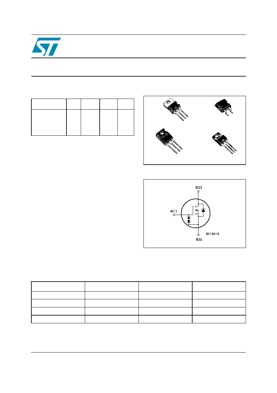
Order codes
Package
Internal schematic diagram
Type
V
DSS
R
DS(on)
I
D
Pw
STB9NK90Z
STW9NK90Z
STP9NK90Z
STF9NK90Z
900 V
900 V
900 V
900 V
<1.3
<1.3
<1.3
<1.3
8 A
8 A
8 A
8 A
160 W
160 W
160 W
40 W
1
2
3
1
2
3
TO-220
TO-220FP
1
3
TO-247
D≤PAK
1
2
3
Sales Type
Marking
Package
Packaging
STB9NK90Z
B9NK90Z
D≤PAK
TAPE & REEL
STF9NK90Z
F9NK90Z
TO-220FP
TUBE
STP9NK90Z
P9NK90Z
TO-220
TUBE
STW9NK90Z
W9NK90Z
TO-247
TUBE
www.st.com
1 Electrical ratings
STB9NK90Z - STF9NK90Z - STP9NK90Z - STW9NK90Z
2/15
1 Electrical
ratings
Table 1.
Absolute maximum ratings
Table 2.
Thermal data
Table 3.
Avalanche characteristics
Symbol
Parameter
Value
Unit
TO-220/D≤PAK/
TO-247
TO-220FP
V
DS
Drain-Source Voltage (V
GS
= 0)
900
V
V
DGR
Drain-gate Voltage (R
GS
= 20k
)
900
V
V
GS
Gate-Source Voltage
± 30
V
I
D
Drain Current (continuous) at T
C
= 25∞C
8
8 (
Note
1)
A
I
D
Drain Current (continuous) at T
C
= 100∞C
5
5 (
Note
1)
A
I
DM
Note
2
Drain Current (pulsed)
32
32 (
Note
1)
A
P
TOT
Total Dissipation at T
C
= 25∞C
160
40
W
Derating Factor
1.28
0.32
W/∞C
Vesd(G-S)
G-S ESD (HBM C=100pF, R=1.5k
)
4
KV
dv/dt
Note
3 Peak Diode Recovery voltage slope
4.5
V/ns
V
ISO
Insulation Withstand Volatge (DC)
--
2500
V
T
j
T
stg
Operating Junction Temperature
Storage Temperature
-55 to 150
∞C
TO-220/
D≤PAK
TO-220FP
TO-247
Unit
Rthj-case
Thermal Resistance Junction-case Max
0.78
3.1
0.78
∞C/W
Rthj-amb
Thermal Resistance Junction-amb Max
62.5
50
∞C/W
T
l
Maximum Lead Temperature For Soldering
Purpose
300
∞C
Symbol
Parameter
Max Value
Unit
I
AR
Avalanche Current, repetitive or
Not-Repetitive (pulse width limited by Tj max)
8
A
E
AS
Single Pulse Avalanche Energy
(starting Tj=25∞C, I
D
=I
AR
, V
DD
= 50V)
300
mJ
STB9NK90Z - STF9NK90Z - STP9NK90Z - STW9NK90Z
2 Electrical characteristics
3/15
2 Electrical
characteristics
(T
CASE
= 25 ∞C unless otherwise specified)
Table 4.
On/off states
Table 5.
Dynamic
Table 6.
Switching times
Symbol
Parameter
Test Conditions
Min.
Typ.
Max.
Unit
V
(BR)DSS
Drain-Source Breakdown
Voltage
I
D
= 1 mA, V
GS
= 0
900
V
I
DSS
Zero Gate Voltage Drain
Current (V
GS
= 0)
V
DS
= Max Rating,
V
DS
= Max Rating,Tc=125∞C
1
50
µA
I
GSS
Gate Body Leakage Current
(V
DS
= 0)
V
GS
= ±20 V, V
DS
= 0
±
10
µA
V
GS(th)
Gate Threshold Voltage
V
DS
= V
GS
, I
D
= 100 µA
3
3.75
4.5
V
R
DS(on)
Static Drain-Source On
Resistance
V
GS
= 10 V, I
D
= 3.6 A
1.1
1.3
Symbol
Parameter
Test Conditions
Min.
Typ.
Max.
Unit
g
fs
Note
4
Forward Transconductance
V
DS
=15V, I
D
= 3.6 A
5.75
S
C
iss
C
oss
C
rss
Input Capacitance
Output Capacitance
Reverse Transfer Capacitance
V
DS
=25V, f=1 MHz, V
GS
=0
2115
190
40
pF
pF
pF
C
oss eq.
Note
5
Equivalent Ouput Capacitance V
GS
=0, V
DS
=0V to 720V
115
pF
Q
g
Q
gs
Q
gd
Total Gate Charge
Gate-Source Charge
Gate-Drain Charge
V
DD
=720V, I
D
= 8A
V
GS
=10V
(see Figure 19)
72
14
38
100
nC
nC
nC
Symbol
Parameter
Test Conditions
Min.
Typ.
Max.
Unit
t
d(on)
t
r
Turn-on Delay Time
Rise Time
V
DD
=450 V, I
D
=4A,
R
G
=4.7
,
V
GS
=10V
(see Figure 20)
22
13
ns
ns
t
d(off)
t
f
Turn-off Delay Time
Fall Time
V
DD
=450 V, I
D
=4A,
R
G
=4.7
,
V
GS
=10V
(see Figure 20)
55
28
ns
ns
t
r(Voff)
t
f
t
c
Off-voltage Rise Time
Fall Time
Cross-over Time
V
DD
=720 V, I
D
=8A,
R
G
=4.7
,
V
GS
=10V
(see Figure 20)
53
11
22
ns
ns
ns

2 Electrical characteristics
STB9NK90Z - STF9NK90Z - STP9NK90Z - STW9NK90Z
4/15
Table 7.
Gate-source zener diode
Table 8.
Source drain diode
(1)Limited only by maximum temperature allowed
(2) Pulse width limited by safe operating area
(3) I
SD
10A, di/dt
200A/µs, V
DD
V
(BR)DSS
, T
j
T
JMAX
(4) Pulsed: pulse duration = 300µs, duty cycle 1.5%
(5) C
oss eq.
is defined as a constant equivalent capacitance giving the same charging time as C
oss
when V
DS
increases from 0
to 80%
(6) The built-in back-to-back Zener diodes have specifically been designed to enhance not only the device's ESD capability,
but also to make them safely absorb possible voltage transients that may occasionally be applied from gate to source. In
this respect the Zener voltage is appropriate to achieve an efficient and cost-effective intervention to protect the device's
integrity. These integrated Zener diodes thus avoid the usage of external components.
Symbol
Parameter
Test Conditions
Min.
Typ.
Max.
Unit
BV
GSO
Note
6
Gate-Source
Breakdown Voltage
Igs=±1mA
(Open Drain)
30
V
Symbol
Parameter
Test Conditions
Min.
Typ.
Max.
Unit
I
SD
I
SDM
Note
2
Source-drain Current
Source-drain Current (pulsed)
8
32
A
A
V
SD
Note
4
Forward on Voltage
I
SD
=8 A, V
GS
=0
1.6
V
t
rr
Q
rr
I
RRM
Reverse Recovery Time
Reverse Recovery Charge
Reverse Recovery Current
I
SD
=8A, di/dt = 100A/µs,
V
DD
=50 V, Tj=150∞C
950
10
21
ns
µC
A

STB9NK90Z - STF9NK90Z - STP9NK90Z - STW9NK90Z
2 Electrical characteristics
5/15
2.1 Electrical
characteristics
(curves)
Figure 1.
Safe Operating Area for
TO-220/D≤PAK
Figure 2.
Thermal Impedanc for
TO-220/D≤PAK
Figure 3.
Safe Operating Area for TO-220FP
Figure 4.
Thermal Impedance for TO-220FP
Figure 5.
Safe Operating Area for TO-247
Figure 6.
Thermal Impedance for TO-247