 | –≠–ª–µ–∫—Ç—Ä–æ–Ω–Ω—ã–π –∫–æ–º–ø–æ–Ω–µ–Ω—Ç: GS100T300 | –°–∫–∞—á–∞—Ç—å:  PDF PDF  ZIP ZIP |

GS70/100T300 Family
70W/100W DC-DC CONVERTERS FAMILY
June 1994
1/10
Type
V
i
V
o
I
o
GS70T300-3.5
200 to 400 V
3,5 V
20 A
GS100T300-5
200 to 400 V
5,2 V
20 A
GS100T300-12
200 to 400 V
12,0 V
8,3 A
GS100T300-15
200 to 400 V
15,0 V
6,6 A
GS100T300-24
200 to 400 V
24,0 V
4,2 A
GS100T300-48
200 to 400 V
48,0 V
2,0 A
FEATURES
High input voltage range bus: 200 to 400Vdc
UL, TUV approved
High output power (up to 100W)
High efficiency (80% min. on GS100T300-5 mod-
ule)
Output voltages range: 3.5-5.2-12-15-24and 48V
Output voltage adjustable by external pin
Remote load voltage sense compensation
Output short-circuit protection
Output overvoltage protection
Undervoltage lock-out
Minimal overshoot during load transients
3750V
RMS
input to output isolation voltage
Internal input and output filtering
Softstart
PCB or chassis mountable
Mechanical Dimensions 101,6
∑
50,8
∑
20 mm
(4,00
∑
2,00
∑
0,79 inches)
DESCRIPTION
The GS70/100T300 family includes 70/100W DC-
DC converters used to generate isolated output
voltages with an output current up to 20A from a
wide range input voltage (200 to 400Vdc).
All the GS70/10 0T300 family modules require an
external fuse (1 Amps.) on the input side.

2/10
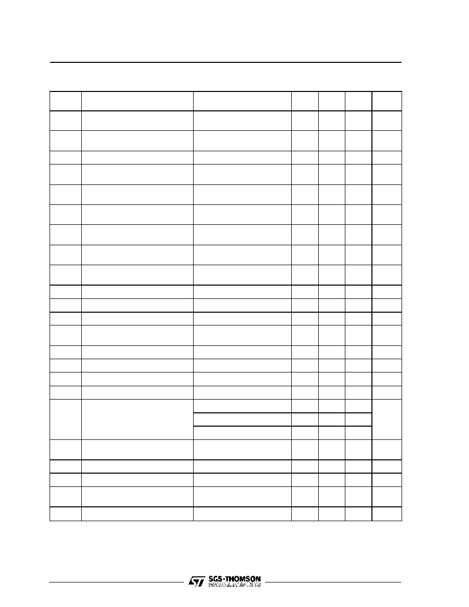
GS70T300-3.5 ELECTRICAL CHARACTERISTICS (T
amb
= 25
∞
C unless otherwise specified)
Symbol
Parameter
Test Conditions
Min
Typ
Max
Unit
Vi
Input Voltage
Vo = 3.5V
Io = 0 to 20A
(Operating Conditions)
200
300
400
V
DC
Qi
Inrush Charge
Vi = 400V
Io = 20A
40
∑
10
-6
C
Pi
Input Power
Vi = 300V
Io = 0A (No Load)
2.5
W
Vo
Output Voltage
Vi = 200 to 400V
Io = 0 to 20A
3.43
3.5
3.57
V
Vo
Output Voltage Range
Vi = 200 to 400V
Io = 0 to 20A (see fig. 2)
1.75
3.5
V
Vorn
Output Ripple and
Noise Voltage
Vi = 300V
Io = 20A
BW = 0 to 20Mhz
35
40
mVpp
Vol
Output Overvoltage
Limit Initiation
Vi = 200 to 400V
Io = 0 to 20A
1.2
∑
Vo
V
V
OL
Line Regulation
Vi = 200 to 400V
Io = 20A
±
0.1
%
V
OO
Load Regulation
Vi = 300V
Io = 0 to 20A
±
0.1
%
Vo
Total Remote Sense Compensation
Vi = 200 to 400V
0.6
V
Vo
Peak Load Transient Response
Vi = 300V
Io = 10A
500
mVp
SVR
Supply Voltage Rejection
f = 100Hz
55
dB
Io
Output Current
Vi = 200 to 400V
Vo = 3.3V
0
20
A
IoI
Overcurrent Limit Initiation
Vi = 300V
21
23
25
A
Iosc
Shortcircuit Output Current
Vi = 300V
18
23
28
A
ts
Load Transient Settling Time
Vi = 300V
Io = 10A
300
µ
s
ton
Turn-on Time
Vi = 200V
Io = 20A
6
10
ms
Vis
Isolation Voltage
Input to Output
3750
V
RMS
Input to Baseplate
2500
Output to Baseplate
500
fs
Switching Frequency
Vi = 200 to 400V
Io = 0 to 20A
150
kHz
Efficiency
Vi = 300V
Io = 20A
78
79
%
Rth
Thermal Resistance
Baseplate to Ambient
7.5
∞
C/W
Tcop
Operating Case
Temperature Range
0
+70
∞
C
Tstg
Storage Temperature Range
≠ 40
+100
∞
C
GS70/100T300 Family

Symbol
Parameter
Test Conditions
Min
Typ
Max
Unit
Vi
Input Voltage
Vo = 5V
Io = 0 to 20A
(Operating Conditions)
200
300
400
V
DC
Qi
Inrush Charge
Vi = 400V
Io = 20A
40
∑
10
-6
C
Pi
Input Power
Vi = 300V
Io = 0A (No Load)
2.5
W
Vo
Output Voltage
Vi = 200 to 400V
Io = 0 to 20A
5.09
5.20
5.30
V
Vo
Output Voltage Range
Vi = 200 to 400V
Io = 0 to 20A (see fig. 2)
2.6
5.20
V
Vorn
Output Ripple and
Noise Voltage
Vi = 300V
Io = 20A
BW = 0 to 20Mhz
40
50
mVpp
Vol
Output Overvoltage
Limit Initiation
Vi = 200 to 400V
Io = 0 to 20A
1.2
∑
Vo
V
V
OL
Line Regulation
Vi = 200 to 400V
Io = 20A
±
0.1
%
V
OO
Load Regulation
Vi = 300V
Io = 0 to 20A
±
0.1
%
Vo
Total Remote Sense Compensation
Vi = 200 to 400V
0.6
V
Vo
Peak Load Transient Response
Vi = 300V
Io = 1A
500
mVp
SVR
Supply Voltage Rejection
f = 100Hz
55
dB
Io
Output Current
Vi = 200 to 400V
Vo = 5V
0
20
A
IoI
Overcurrent Limit Initiation
Vi = 300V
21
23
25
A
Iosc
Shortcircuit Output Current
Vi = 300V
18
23
28
A
ts
Load Transient Settling Time
Vi = 300V
Io = 1A
300
µ
s
ton
Turn-on Time
Vi = 200V
Io = 20A
6
10
ms
Vis
Isolation Voltage
Input to Output
3750
V
RMS
Output to Baseplate
500
Input to Baseplate
2500
fs
Switching Frequency
Vi = 200 to 400V
Io = 0 to 20A
150
kHz
Efficiency
Vi = 300V
Io = 20A
80
81
%
Rth
Thermal Resistance
Baseplate to Ambient
7.5
∞
C/W
Tcop
Operating Case
Temperature Range
0
+70
∞
C
Tstg
Storage Temperature Range
≠ 40
+100
∞
C
GS100T300-5 ELECTRICAL CHARACTERISTICS (T
amb
= 25
∞
C unless otherwise specified)
3/10
GS70/100T300 Family
Symbol
Parameter
Test Conditions
Min
Typ
Max
Unit
Vi
Input Voltage
Vo = 12V
Io = 0 to 8.3A
(Operating Conditions)
200
300
400
V
DC
Qi
Inrush Charge
Vi = 400V
Io = 8.3A
40
∑
10
-6
C
Pi
Input Power
Vi = 300V
Io = 0A (No Load)
2.5
W
Vo
Output Voltage
Vi = 200 to 400V
Io = 0 to 8.3A
11.76
12.00
12.24
V
Vo
Output Voltage Range
Vi = 200 to 400V
Io = 0 to 8.3A (see fig. 2)
6.0
13.2
V
Vorn
Output Ripple and
Noise Voltage
Vi = 300V
Io = 8.3A
BW = 0 to 20Mhz
100
120
mVpp
Vol
Output Overvoltage
Limit Initiation
Vi = 200 to 400V
Io = 0 to 8.3A
1.2
∑
Vo
V
V
OL
Line Regulation
Vi = 200 to 400V
Io = 8.3A
±
0.1
%
V
OO
Load Regulation
Vi = 300V
Io = 0 to 8.3A
±
0.1
%
Vo
Total Remote Sense Compensation
Vi = 200 to 400V
0.6
V
Vo
Peak Load Transient Response
Vi = 300V
Io = 4A
500
mVp
SVR
Supply Voltage Rejection
f = 100Hz
45
dB
Io
Output Current
Vi = 200 to 400V
Vo = 12V
0
8.3
A
IoI
Overcurrent Limit Initiation
Vi = 300V
8.8
9.1
11.0
A
Iosc
Shortcircuit Output Current
Vi = 300V
7.5
9.0
11.0
A
ts
Load Transient Settling Time
Vi = 300V
Io = 4A
300
µ
s
ton
Turn-on Time
Vi = 200V
Io = 8.3A
6
10
ms
Vis
Isolation Voltage
Input to Output
3750
V
RMS
Input to Baseplate
2500
Output to Baseplate
500
fs
Switching Frequency
Vi = 200 to 400V
Io = 0 to 8.3A
150
kHz
Efficiency
Vi = 300V
Io = 8.3A
83
84
%
Rth
Thermal Resistance
Baseplate to Ambient
7.5
∞
C/W
Tcop
Operating Case
Temperature Range
0
+70
∞
C
Tstg
Storage Temperature Range
≠ 40
+100
∞
C
GS100T300-12ELECTRICAL CHARACTERISTICS (T
amb
= 25
∞
C unless otherwise specified)
4/10
GS70/100T300 Family

Symbol
Parameter
Test Conditions
Min
Typ
Max
Unit
Vi
Input Voltage
Vo = 15V
Io = 0 to 6.6A
(Operating Conditions)
200
300
400
V
DC
Qi
Inrush Charge
Vi = 400V
Io = 6.6A
40
∑
10
-6
C
Pi
Input Power
Vi = 300V
Io = 0A (No Load)
2.5
W
Vo
Output Voltage
Vi = 200 to 400V
Io = 0 to 6.6A
14.7
15.0
15.3
V
Vo
Output Voltage Range
Vi = 200 to 400V
Io = 0 to 6.6A (see fig. 2)
7.5
16.5
V
Vorn
Output Ripple and
Noise Voltage
Vi = 300V
Io = 6.6A
BW = 0 to 20Mhz
110
150
mVpp
Vol
Output Overvoltage
Limit Initiation
Vi = 200 to 400V
Io = 0 to 6.6A
1.2
∑
Vo
V
V
OL
Line Regulation
Vi = 200 to 400V
Io = 6.6A
±
0.1
%
V
OO
Load Regulation
Vi = 300V
Io = 0 to 6.6A
±
0.1
%
Vo
Total Remote Sense Compensation
Vi = 200 to 400V
0.6
V
Vo
Peak Load Transient Response
Vi = 300V
Io = 3.3A
500
mVp
SVR
Supply Voltage Rejection
f = 100Hz
45
dB
Io
Output Current
Vi = 200 to 400V
Vo = 15V
0
6.6
A
IoI
Overcurrent Limit Initiation
Vi = 300V
7.1
7.5
8.0
A
Iosc
Shortcircuit Output Current
Vi = 300V
6.5
8.0
10.0
A
ts
Load Transient Settling Time
Vi = 300V
Io = 3.3A
300
µ
s
ton
Turn-on Time
Vi = 200V
Io = 6.6A
6
10
ms
Vis
Isolation Voltage
Input to Output
3750
V
RMS
Input to Baseplate
2500
Output to Baseplate
500
fs
Switching Frequency
Vi = 200 to 400V
Io = 0 to 6.6A
150
kHz
Efficiency
Vi = 300V
Io = 6.6A
84
85
%
Rth
Thermal Resistance
Baseplate to Ambient
7.5
∞
C/W
Tcop
Operating Case
Temperature Range
0
+70
∞
C
Tstg
Storage Temperature Range
≠ 40
+100
∞
C
GS100T300-15ELECTRICAL CHARACTERISTICS (T
amb
= 25
∞
C unless otherwise specified)
5/10
GS70/100T300 Family

Symbol
Parameter
Test Conditions
Min
Typ
Max
Unit
Vi
Input Voltage
Vo = 24V
Io = 0 to 4.2A
(Operating Conditions)
200
300
400
V
DC
Qi
Inrush Charge
Vi = 400V
Io = 4.2A
40
∑
10
-6
C
Pi
Input Power
Vi = 300V
Io = 0A (No Load)
2.5
W
Vo
Output Voltage
Vi = 200 to 400V
Io = 0 to 4.2A
23.5
24.0
24.5
V
Vo
Output Voltage Range
Vi = 200 to 400V
Io = 0 to 4.2A (see fig. 2)
12.0
26.4
V
Vorn
Output Ripple and
Noise Voltage
Vi = 300V
Io = 4.2A
BW = 0 to 20Mhz
200
240
mVpp
Vol
Output Overvoltage
Limit Initiation
Vi = 200 to 400V
Io = 0 to 4.2A
1.2
∑
Vo
V
V
OL
Line Regulation
Vi = 200 to 400V
Io = 4.2A
±
0.1
%
V
OO
Load Regulation
Vi = 300V
Io = 0 to 4.2A
±
0.1
%
Vo
Total Remote Sense Compensation
Vi = 200 to 400V
0.6
V
Vo
Peak Load Transient Response
Vi = 300V
Io = 2.1A
500
mVp
SVR
Supply Voltage Rejection
f = 100Hz
40
dB
Io
Output Current
Vi = 200 to 400V
Vo = 24V
0
4.2
A
IoI
Overcurrent Limit Initiation
Vi = 300V
4.5
5.0
5.5
A
Iosc
Shortcircuit Output Current
Vi = 300V
3.8
4.5
6.0
A
ts
Load Transient Settling Time
Vi = 300V
Io = 2.1A
300
µ
s
ton
Turn-on Time
Vi = 200V
Io = 4.2A
6
10
ms
Vis
Isolation Voltage
Input to Output
3750
V
RMS
Input to Baseplate
2500
Output to Baseplate
500
fs
Switching Frequency
Vi = 200 to 400V
Io = 0 to 4.2A
150
kHz
Efficiency
Vi = 300V
Io = 4.2A
84
85
%
Rth
Thermal Resistance
Baseplate to Ambient
7.5
∞
C/W
Tcop
Operating Case
Temperature Range
0
+70
∞
C
Tstg
Storage Temperature Range
≠ 40
+100
∞
C
GS100T300-24ELECTRICAL CHARACTERISTICS (T
amb
= 25
∞
C unless otherwise specified)
6/10
GS70/100T300 Family

Symbol
Parameter
Test Conditions
Min
Typ
Max
Unit
Vi
Input Voltage
Vo = 48V
Io = 0 to 2.1A
(Operating Conditions)
200
300
400
V
DC
Qi
Inrush Charge
Vi = 400V
Io = 2.1A
40
∑
10
-6
C
Pi
Input Power
Vi = 300V
Io = 0A (No Load)
2.5
W
Vo
Output Voltage
Vi = 200 to 400V
Io = 0 to 2.1A
47.04
48.00
48.96
V
Vo
Output Voltage Range
Vi = 200 to 400V
Io = 0 to 2.1A (see fig. 2)
24.0
52.8
V
Vorn
Output Ripple and
Noise Voltage
Vi = 300V
Io = 2.1A
BW = 0 to 20Mhz
400
500
mVpp
Vol
Output Overvoltage
Limit Initiation
Vi = 200 to 400V
Io = 0 to 2.1A
1.2
∑
Vo
V
V
OL
Line Regulation
Vi = 200 to 400V
Io = 2.1A
±
0.1
%
V
OO
Load Regulation
Vi = 300V
Io = 0 to 2.1A
±
0.1
%
Vo
Total Remote Sense Compensation
Vi = 200 to 400V
0.6
V
Vo
Peak Load Transient Response
Vi = 300V
Io = 1A
500
mVp
SVR
Supply Voltage Rejection
f = 100Hz
35
dB
Io
Output Current
Vi = 200 to 400V
Vo = 48V
0
2
A
IoI
Overcurrent Limit Initiation
Vi = 300V
2.1
2.3
2.5
A
Iosc
Shortcircuit Output Current
Vi = 300V
1.8
2.3
2.8
A
ts
Load Transient Settling Time
Vi = 300V
Io = 1A
300
µ
s
ton
Turn-on Time
Vi = 200V
Io = 2.1A
6
10
ms
Vis
Isolation Voltage
Input to Output
3750
V
RMS
Input to Baseplate
2500
Output to Baseplate
500
fs
Switching Frequency
Vi = 200 to 400V
Io = 0 to 2.1A
150
kHz
Efficiency
Vi = 300V
Io = 2.1A
84
85
%
Rth
Thermal Resistance
Baseplate to Ambient
7.5
∞
C/W
Tcop
Operating Case
Temperature Range
0
+70
∞
C
Tstg
Storage Temperature Range
≠ 40
+100
∞
C
GS100T300-48ELECTRICAL CHARACTERISTICS (T
amb
= 25
∞
C unless otherwise specified)
7/10
GS70/100T300 Family
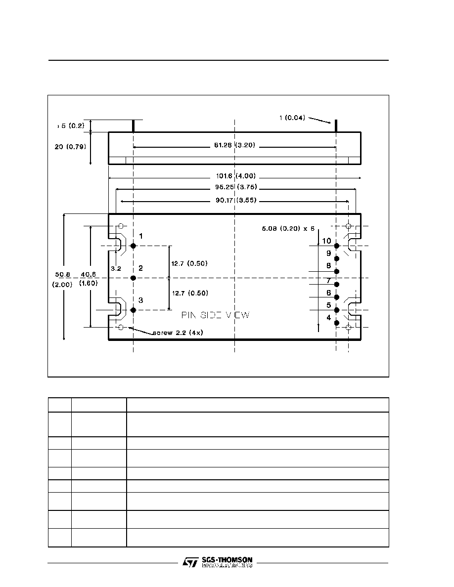
Package R; dimensions in mm (inches)
CONNECTION DIAGRAM AND MECHANICAL DATA
Figure 1.
8/10
PIN DESCRIPTION
Pin
Function
Description
1
ENABLE
The converter is ON (Enable) when the voltage applied to this pin with reference to pin 2 is
lower than 1.2V. The converter is OFF (Inhibit) for a control voltage in the range of 2.1 to
5V. When the pin is unconnected the converter is OFF (Inhibit).
2
- Vin
Negative input voltage.
3
+ Vin
Positive input voltage. Unregulated input voltage in the range of 200 to 400Vdc must be
applied between pin 2-3.
4,5
+ Vo
+Vo output voltage.
6,7
- Vo
+Vo output voltage return.
8
+ SENSE
Senses the remote load high side. To be connected to pins 4,5 when remote sense is not
used.
9
- SENSE
Senses the remote load return. To be connected to pins 6,7 when remote sense is not
used.
10
ADJ
Adjust output voltage pin. A voltage generator between the ADJ. pin and -SENSE pin sets
the Vo. When unconnected Vo is at nominal value (see fig. 2).
GS70/100T300 Family
9/10
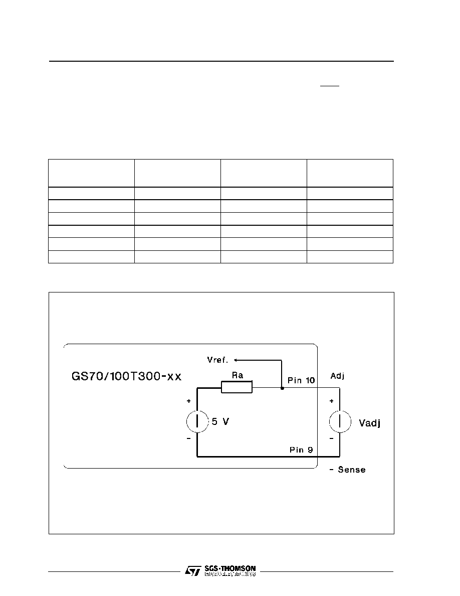
ADJUSTMENT OF THE OUTPUT VOLTAGE
The output voltage can be fixed following the indi-
cations given in fig. 2. The external reference volt-
age Vadj can be calculated using the following
formula:
V
adj
= 5
∑
V
o
V
nom
The Vout and Vadj ranges are given in the following
table:
Table 1: Output voltage generation with external voltage generator
Type
Nominal Output
Voltage (V)
Output Voltage
Range (V
out)
External Voltage
Generator allowed
Range (V
adj
)
GS70T300-3.5
3.5
1.75 to 3.50
2.5 to 5.0
GS100T300-5
5.2
2.60 to 5.20
2.5 to 5.0
GS100T300-12
12.0
6.00 to 13.20
2.5 to 5.5
GS100T300-15
15.0
7.50 to 16.50
2.5 to 5.5
GS100T300-24
24.0
12.00 to 26.40
2.5 to 5.5
GS100T300-48
48.0
24.00 to 52.80
2.5 to 5.5
Figure 2. Output voltage adjustment
GS70/100T300 Family
10/10
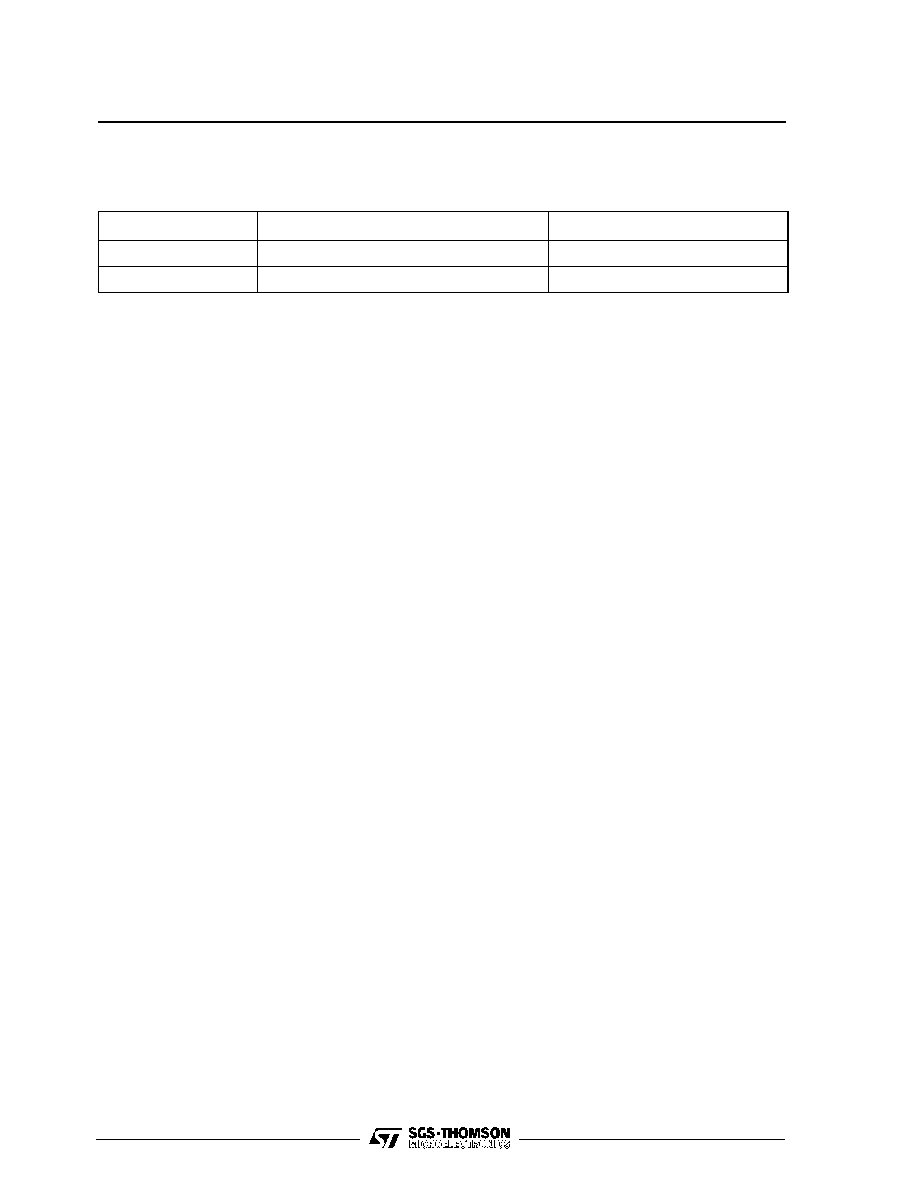
Safety approvals
The converter is agency certified to the following safety requirements.
Agency
Requirements
License Number
UL
UL-STD-1950
E141284
TUV
EN 60950
R 9371740.1
Information furnished is believed to be accurate and reliable. However, SGS-THOMSON Microelectronics assumes no responsibility for the
consequences of use of such information nor for any infringement of patents or other rights of third parties which may result from its use. No
license is granted by implication or otherwise under any patent or patent rights of SGS-THOMSON Microelectronics. Specification mentioned
in this publication are subject to change without notice. This publication supersedes and replaces all information previously supplied.
SGS-THOMSON Microelectronics products are not authorized for use as critical components in life support devices or systems without express
written approval of SGS-THOMSON Microelectronics.
©
1994 SGS-THOMSON Microelectronics ≠ All Rights Reserved
Æ
UL is a registered trademark of UNDERWRITERS LABORATORIES inc.
Æ
TUV is a registered trademark of TUV Rheinland.
SGS-THOMSON Microelectronics GROUP OF COMPANIES
Australia - Brazil - China - France - Germany - Hong Kong - Italy - Japan - Korea - Malaysia - Malta - Morocco - The Netherlands -
Singapore - Spain - Sweden - Switzerland - Taiwan - Thailand - United Kingdom - U.S.A.
Æ
UL is a registered trademark of UNDER WRITERS LABORATORIES inc.
Æ
TUV is a registered trademark of TUV Rheinland.
GS70/100T300 Family